


 The Right Approach: I Hear the Train A Comin'
 It’s Only Common Sense: OCCAM—the Time Is Now
 Marcy's Musings: The Growing Industry
Flexible Circuits for 3D Printing
April 29, 2019 | DESYEstimated reading time: 3 minutes
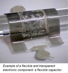
A research cooperation between the University of Hamburg and DESY has developed a process suitable for 3D printing that can be used to produce transparent and mechanically flexible electronic circuits. The electronics consists of a mesh of silver nanowires that can be printed in suspension and embedded in various flexible and transparent plastics (polymers). This technology can enable new applications such as printable light-emitting diodes, solar cells or tools with integrated circuits, as Tomke Glier from the University of Hamburg and her colleagues report in the journal Scientific Reports. The researchers are demonstrating the potential of their process with a flexible capacitor, among other things.
“The aim of this study was to functionalize 3D-printable polymers for different applications,” reports Michael Rübhausen from the Center for Free-Electron Laser Science (CFEL), a cooperation between DESY, the University of Hamburg and the Max Planck Society. “With our novel approach, we want to integrate electronics into existing structural units and improve components in terms of space and weight.” The physics professor from the University of Hamburg led the project together with DESY researcher Stephan Roth, who is also professor at the Royal Institute of Technology in Stockholm. Using the bright X-ray light from DESY's research light source PETRA III and other measuring methods, the team has precisely analyzed the properties of the nanowires in the polymer.
“At the heart of the technology are silver nanowires, which form a conductive mesh,” explains Glier. The silver wires are typically several tens of nanometers (millionths of a millimeter) thick and 10 to 20 micrometers (thousandths of a millimeter) long. The detailed X-ray analysis shows that the structure of the nanowires in the polymer is not changed, but that the conductivity of the mesh even improves thanks to the compression by the polymer, as the polymer contracts during the curing process.
The silver nanowires are applied to a substrate in suspension and dried. “For cost reasons, the aim is to achieve the highest possible conductivity with as few nanowires as possible. This also increases the transparency of the material,” explains Roth, head of the P03 measuring station at DESY's X-ray light source PETRA III, where the X-ray investigations took place. “In this way, layer by layer, a conductive path or surface can be produced.” A flexible polymer is applied to the conductive tracks, which in turn can be covered with conductive tracks and contacts. Depending on the geometry and material used, various electronic components can be printed in this way.
In this paper, the researchers produced a flexible capacitor. “In the laboratory, we carried out the individual work steps in a layering process, but in practice they can later be completely transferred to a 3D printer,” explains Glier. “However, the further development of conventional 3D printing technology, which is usually optimized for individual printing inks, is also essential for this. In inkjet-based processes, the print nozzles could be clogged by the nanostructures,” notes Rübhausen.
In the next step, the researchers now want to test how the structure of the conductive paths made of nanowires changes under mechanical stress. “How well does the wire mesh hold together during bending? How stable does the polymer remain,” said Roth, referring to typical questions. “X-ray investigation is very suitable for this because it is the only way we can look into the material and analyze the conductive paths and surfaces of the nanowires.”
Researchers from the University of Hamburg, the Royal Institute of Technology in Stockholm, the Wallenberg Centre for Wood Science in Stockholm, the Max Planck Institute for the Structure and Dynamics of Matter in Hamburg and DESY were involved in the work.
Share on:


Suggested Items
Koh Young Showcases Award-winning Inspection Solutions at SMTconnect with SmartRep in Hall 4A.225
04/25/2024 | Koh Young TechnologyKoh Young Technology, the industry leader in True 3D measurement-based inspection solutions, will showcase an array of award-winning inspection and measurement solutions at SMTconnect alongside its sales partner, SmartRep, in booth 4A.225 at NürnbergMesse from June 11-13, 2023. The following offers a glimpse into what Koh Young will present at the tradeshow:
Real Time with… IPC APEX EXPO 2024: Plasmatreat: Innovative Surface Preparation Solutions
04/25/2024 | Real Time with...IPC APEX EXPOIn this interview, Editor Nolan Johnson speaks with Hardev Grewal, CEO and president of Plasmatreat, a developer of atmospheric plasma solutions. Plasmatreat uses clean compressed air and electricity to create plasma, offering environmentally friendly methods for surface preparation. Their technology measures plasma density for process optimization and can remove organic micro-contamination. Nolan and Hardev also discuss REDOX-Tool, a new technology for removing metal oxides.
Nanotechnology Market to Surpass $53.51 Billion by 2031
04/25/2024 | PRNewswireSkyQuest projects that the nanotechnology market will attain a value of USD 53.51 billion by 2031, with a CAGR of 36.4% over the forecast period (2024-2031).
Cadence, TSMC Collaborate on Wide-Ranging Innovations to Transform System and Semiconductor Design
04/25/2024 | Cadence Design SystemsCadence Design Systems, Inc. and TSMC have extended their longstanding collaboration by announcing a broad range of innovative technology advancements to accelerate design, including developments ranging from 3D-IC and advanced process nodes to design IP and photonics.
SMC Korea 2024 to Highlight Semiconductor Materials Trends and Innovations on Industry’s Path to $1 Trillion
04/24/2024 | SEMIWith Korea a major consumer of semiconductor materials and advanced materials a key driver of innovation on the industry’s path to $1 trillion, industry leaders and experts will gather at SMC (Strategic Materials Conference) Korea 2024 on May 29 at the Suwon Convention Center in Gyeonggi-do, South Korea to provide insights into the latest materials developments and trends. Registration is open.