


 It’s Only Common Sense: OCCAM—the Time Is Now
 Marcy's Musings: The Growing Industry
 Dan’s Biz Bookshelf: Seeing the How
Researchers Create ‘Force Field’ for Super Materials
May 9, 2019 | University of SurreyEstimated reading time: 1 minute
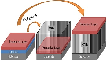
When curved and rolled into cylinders, thin graphene layers form CNT structures which can be a thousandth of the diameter of human hair. Both graphene and CNTs possess extraordinary properties such as extreme electrical conduction, or 100 times the strength of high tensile steel. Although widely regarded as the key to developing various future technologies such as batteries and supercapacitor, growth of graphene and CNTs are plagued with environmental ‘poisoning’ to the catalyst which causes poor conductivity and reliability issues.
In a paper published by the journal Carbon, researchers from the University of Surrey detail their new method for covering the catalyst by using a protective layer that is configured to allow carbon diffusion and therefore can be used to protect the catalyst from environmental contamination. The technique allows the catalyst to be transported, stored or accurately calibrated for future use.
Professor Ravi Silva, Director of Advanced Technology Institute at the University of Surrey, said: “The protective catalyst technique provides a breakthrough in terms of usability and industrial applicability of carbon nanomaterials. For example, the poisoning of the catalyst by environmental contamination such as oxidation and unwanted etching of the thin catalyst film during reactive ion etching or wet-etching can now be prevented.”
Lead author of the study, Dr Muhammad Ahmad from the University of Surrey, said: “The age-old problem of poor attachment of the carbon nano-materials to the substrate has now been solved using this unique technique. By fine tuning the thickness of the protective layer, accurate control of the carbon supply to the catalyst is achieved to grow selected numbers of graphene layers or precise CNT films.”
“We hope that our research will free fellow scientists to unlock the incredible potential of carbon nanomaterials and I would not be surprised to see advances in areas such as sensor, battery and supercapacitor technologies in the very near future.”
Share on:


Suggested Items
SCHMID Group to Exhibit at productronica
11/07/2023 | SCHMID GroupThe SCHMID Group, a global solution provider for the high-tech electronics, photovoltaics, glass and energy systems industries, will be exhibiting at productronica in Munich from November 14 – 17, 2023.
Sigma Mecer: Turning Copper ‘Green’
10/05/2023 | Nolan Johnson, PCB007 MagazineAndreas Littorin is CEO at Sigma Engineering AB. The company has been manufacturing equipment for the PCB industry for 45 years, mainly a mature product for copper recycling of alkaline and acidic etchants in the PCB manufacturing process.
Smart Factory Insights: The Smart Business Case for Local PCB Manufacturing
09/27/2023 | Michael Ford -- Column: Smart Factory InsightsThe PCB has become a neglected component from the Smart assembly manufacturing perspective, wrongly regarded as just a “given” material. We need to put it right. PCB manufacturing needs to become Smart in order to make the local fabrication business model work as part of the holistic electronics’ “smarter, secure, and sustainable” approach—what I’m calling the new three Ss of manufacturing.
Atotech to Participate at KPCA Show 2023 in Seoul, South Korea
08/28/2023 | AtotechMKS’ Atotech will participate at this year’s KPCA Show 2023 in Seoul, South Korea, which will be held at Incheon Songdo Convensia from September 6-8, 2023.
Connect the Dots: Best Drilling Practices for Better PCB Manufacturing
09/05/2023 | Matt Stevenson -- Column: Connect the DotsDrilling is one of the most fundamental steps in the printed circuit board manufacturing process. Until the advent of the through-hole, PCBs were all single-sided with traces and components located on one side. With double-sided and multilayered boards so common now, a PCB without holes doesn't seem like a PCB at all. The drilling process creates the holes that connect the different layers of the PCB. Those holes allow for the connection of components. In fact, without holes, a double-sided PCB is just a coaster.