


 The Right Approach: I Hear the Train A Comin'
 It’s Only Common Sense: OCCAM—the Time Is Now
 Marcy's Musings: The Growing Industry
DGIST Develops Next Generation Core Semiconductor Technology
May 24, 2019 | DGISTEstimated reading time: 2 minutes
The DGIST Department of Information and Communication Engineering developed a graphene-based high-performance transmission line with an improved operating speed of electrons than using the existing metal in high-frequency. This is expected to contribute greatly to next generation’s high-speed semiconductor and communication device with much faster processing speed than the existing one.
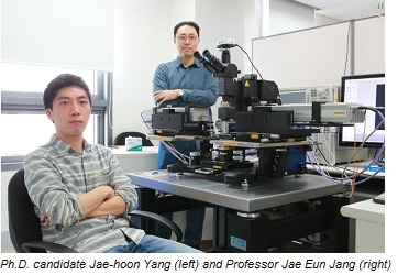
DGIST announced on Thursday, May 2 that Professor Jae Eun Jang’s team researched the high frequency transmission characteristics of single-layer graphene in the Department of Information and Communication Engineering, and developed a high-performance, high-frequency transmission line that induced an increase of device concentration inside graphene. This result showed the characteristics of high frequency transmission with great improvement that can replace the metal used in the existing high-speed semiconductor processing, and its potential use as a transmission line of graphene is expected in the future.
Due to the high-integration and high speed of semiconductor devices, the resistance of metal wire in which signals among devices are transmitted has increased geometrically, reaching the limit of permissible current density. To resolve this issue, carbon-based nano structures such as graphene and carbon nano tube, which are regarded as the substitutes of existing metals, have drawn attention as next generation new materials.
However, graphene has a hexagonal array of carbon, with very thin thickness of 0.3nm, electric conductivity that is 100 times greater than copper, and electron mobility that is 100 times faster than silicon. It has thus been mentioned as an electronic material that can replace the existing metal and semiconductor materials. However, pure graphene has too low device concentration of 1012 cm-2 with thin structural characteristics of nanometer, which results in too high resistance of graphene.
In order to overcome such limitations, Professor Jang’s team conducted a research to improve high frequency transmission characteristics of graphene by enhancing the device concentration inside graphene. By combining graphene and amorphous carbon, the team increased the device concentration of graphene and enhanced the electrical characteristics of graphene. The high frequency transmission of increased graphene was –8dB, which could be comparable to metal nano lines with hundreds of nano size.
The team also proved that defects inside graphene decrease the high frequency transmission of graphene and developed a new, stable doping technique that minimized internal defects. This new doping technique increased the device concentration of graphene by 2x 1013cm-2 and showed stable thermal properties and electrical characteristics.
The high frequency graphene transmission line developed by Professor Jang’s research team displayed high signal transmission efficiency and stable operating characteristics, which can be applied to the metal wiring processing of the existing semiconductor industry as well as next generation integrated circuit.
Professor Jae Eun Jang in the Department of Information and Communication Engineering said “Along with device technology, transmission line is a very important technology in the semiconductor research field. We have developed a core base technology that can enhance the high frequency transmission of graphene that can be used as next generation transmission line. Thanks to the results of convergence research by experts in nano engineering, electronic engineering, and physics, we expect to use the graphene on high-frequency circuit such as MMIC and RFIC.
This research was performed with the support of the Ministry of Science and ICT and basic research project of the National Research Foundation of Korea, and it has been selected to be published as a cover paper of ‘‘Advanced Functional Materials’, a worldwide international journal in material science.
Share on:


Suggested Items
Designer’s Notebook: What Designers Need to Know About Manufacturing, Part 2
04/24/2024 | Vern Solberg -- Column: Designer's NotebookThe printed circuit board (PCB) is the primary base element for providing the interconnect platform for mounting and electrically joining electronic components. When assessing PCB design complexity, first consider the component area and board area ratio. If the surface area for the component interface is restricted, it may justify adopting multilayer or multilayer sequential buildup (SBU) PCB fabrication to enable a more efficient sub-surface circuit interconnect.
Insulectro’s 'Storekeepers' Extend Their Welcome to Technology Village at IPC APEX EXPO
04/03/2024 | InsulectroInsulectro, the largest distributor of materials for use in the manufacture of PCBs and printed electronics, welcomes attendees to its TECHNOLOGY VILLAGE during this year’s IPC APEX EXPO at the Anaheim Convention Center, April 9-11, 2024.
ENNOVI Introduces a New Flexible Circuit Production Process for Low Voltage Connectivity in EV Battery Cell Contacting Systems
04/03/2024 | PRNewswireENNOVI, a mobility electrification solutions partner, introduces a more advanced and sustainable way of producing flexible circuits for low voltage signals in electric vehicle (EV) battery cell contacting systems.
Heavy Copper PCBs: Bridging the Gap Between Design and Fabrication, Part 1
04/01/2024 | Yash Sutariya, Saturn Electronics ServicesThey call me Sparky. This is due to my talent for getting shocked by a variety of voltages and because I cannot seem to keep my hands out of power control cabinets. While I do not have the time to throw the knife switch to the off position, that doesn’t stop me from sticking screwdrivers into the fuse boxes. In all honesty, I’m lucky to be alive. Fortunately, I also have a talent for building high-voltage heavy copper circuit boards. Since this is where I spend most of my time, I can guide you through some potential design for manufacturability (DFM) hazards you may encounter with heavy copper design.
Trouble in Your Tank: Supporting IC Substrates and Advanced Packaging, Part 5
03/19/2024 | Michael Carano -- Column: Trouble in Your TankDirect metallization systems based on conductive graphite or carbon dispersion are quickly gaining acceptance worldwide. Indeed, the environmental and productivity gains one can achieve with these processes are outstanding. In today’s highly competitive and litigious environment, direct metallization reduces costs associated with compliance, waste treatment, and legal issues related to chemical exposure. What makes these processes leaders in the direct metallization space?