


 Marcy's Musings: The Growing Industry
 It’s Only Common Sense: Here’s What To Do After IPC APEX EXPO 2024
 Dan’s Biz Bookshelf: Seeing the How
Imperfection is OK for Better MOFs
May 28, 2019 | KAUSTEstimated reading time: 2 minutes
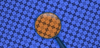
Perfect crystals are not necessarily the most useful. Defects in the ordered crystalline structure of metal-organic frameworks (MOFs) could tailor these versatile materials for specific applications. KAUST researchers have already developed a pioneering method to image the defects using transmission electron microscopy. They now report that creating specific defects, visualizing them, and investigating their chemical effects takes the exploration of MOFs to new levels of detail and control.
MOFs contain regularly spaced metallic clusters connected by carbon-based organic linker groups. Varying the metals in the clusters and the structure of the linkers creates a huge diversity of MOFs with varying pore networks and different chemical properties. Two of the major applications MOFs are being developed for are for use as catalysts and as highly selective gas adsorption and separation materials.
MOFs are one of the hottest areas of chemical research, and KAUST scientists are hard at work to remain in the forefront. The latest advance builds on a long record of discoveries and has involved three KAUST research centers, the KAUST Core labs and collaborators in China and the UK.
"The biggest surprise we are revealing is that there are diverse defects in almost all MOFs, even those that were previously considered to be perfect," says researcher, Yu Han of the KAUST Advanced Membranes and Porous Materials Center.
Han explains that investigating the defects is challenging because MOF crystals are fragile and easily damaged by the electron beams used in conventional electron microscopy. The KAUST team has overcome this problem by using a highly sensitive electron-counting camera, combined with a suite of specially designed image processing methods.
This new ability to peer directly into a MOF at a high level of resolution reveals that two types of defects can coexist, due to missing metallic clusters and missing linkers. "Such details could not be seen prior to our work," says Han.
The researchers also explored creating defects in MOFs with chemical treatment and monitoring how the pattern of defects develops. This demonstrates the potential to fine tune the defects to manipulate the chemical properties of a MOF.
The KAUST team has demonstrated the power of this strategy by finding that a specific MOF with missing cluster defects is more catalytically active than one with missing linker defects.
The researchers are now working to further refine their imaging technique and to apply it to larger crystals. "We hope to disclose more unknowns about MOFs in order to optimize their applications," says Han.
Share on:


Suggested Items
Inkjet Solder Mask ‘Has Arrived’
04/10/2024 | Pete Starkey, I-Connect007I was delighted to be invited to attend an interactive webinar entitled “Solder Mask Coating Made Easy with Additive Manufacturing,” hosted by SUSS MicroTec Netherlands in Eindhoven. The webinar was introduced and moderated by André Bodegom, managing director at Adeon Technologies, and the speakers were Mariana Van Dam, senior product manager PCB imaging solutions at AGFA in Belgium; Ashley Steers, sales manager at Electra Polymers in the UK; and Dr. Luca Gautero, product manager at SUSS MicroTec Netherlands.
NetVia Group Acquires Direct Imaging from Mivatek
04/09/2024 | Miva TechnologiesMiva Technologies is pleased to announce NetVia Group, Irving, TX has acquired a new Miva 2400NG Dual Tray Direct Imaging System with 30-micron capabilities for inner, outer and soldermask imaging.
Teledyne to Acquire Adimec
02/13/2024 | TeledyneTeledyne Technologies Incorporated announced that it has entered into an agreement to acquire Adimec Holding B.V. and its subsidiaries.
Real Time with... productronica 2023: MivaTek Global Advances Technology With High-res Imaging System
12/08/2023 | Real Time with...productronicaMivaTek's Brendan Hogan talks about how the company employs Digitally Adaptive Rasterization Technology (DART) in their high-res imaging equipment. He also shares how the blurred line between semiconductors and microelectronics is driving broader application of the imaging process.
Keysight Enables Validation of Arbe 4D Imaging Radar Chipset
11/30/2023 | Keysight Technologies, Inc.Keysight Technologies, Inc. announces that Arbe has selected the E8719A Radar Target Solution (RTS) to test the Arbe 4D imaging radar chipset for automotive applications.