


 It’s Only Common Sense: OCCAM—the Time Is Now
 Marcy's Musings: The Growing Industry
 Dan’s Biz Bookshelf: Seeing the How
Quantum Information Gets a Boost from Thin-Film Breakthrough
May 30, 2019 | Los Alamos National LaboratoryEstimated reading time: 2 minutes
Efforts to create reliable light-based quantum computing, quantum key distribution for cybersecurity, and other technologies got a boost from a new study demonstrating an innovative method for creating thin films to control the emission of single photons.
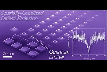
Image Caption: An innovative method for controlling single-photon emission for specific locations in 2D materials may offer a new path toward all-optical quantum computers and other quantum technologies. This image shows a false-color scanning electron micrograph of the array used to create place single-photon sources in epitaxial tungsten diselenide. Inset shows the Hanbury-Brown Twiss interferometry measurement proving quantum emission.
“Efficiently controlling certain thin-film materials so they emit single photons at precise locations—what’s known as deterministic quantum emission—paves the way for beyond-lab-scale quantum materials,” said Michael Pettes, a Los Alamos National Laboratory materials scientist and leader of the multi-institution research team.
The scalability of these two-dimensional, tungsten/selenium thin films makes them potentially useful in processes to manufacture quantum technologies. Single-photon generation is a requirement for all-optical quantum computing and key distribution in quantum communications, and it is crucial for advancing quantum information technologies.
The project, documented as a Featured Article in the journal Applied Physics Letters this week, exploits strain at highly spatially localized and well-separated emission sites, or tips, in a tungsten/selenium film. The team synthesized the film through chemical vapor deposition using a multi-step, diffusion-mediated gas source.
Because the material is very thin, it conforms to the radius of the tips and the material bends towards the substrate by more than a few percent, like someone lying on a bed of nails. The resulting strain is enough to change the electronic structure, but only at the tips. The affected area emits light of a different color and nature than light from the rest of the film.
“While more research is needed to fully understand the role of mechanical deformation in creating these quantum emission sites, we may enable a route to control quantum optical properties by using strain,” Pettes said. “These single-photon sources form the basis for photonics-based, all-optical quantum computing schemes.”
Engineering of quantum emission in 2D materials is still in a very early stage, the authors note. While studies have observed single photons originating from defect structures in these materials, previous work has suggested that non-uniform strain fields might govern the effect. However, the mechanism responsible for this emergent phenomenon remains unclear and is the focus of ongoing work at Los Alamos.
Share on:


Suggested Items
SMC Korea 2024 to Highlight Semiconductor Materials Trends and Innovations on Industry’s Path to $1 Trillion
04/24/2024 | SEMIWith Korea a major consumer of semiconductor materials and advanced materials a key driver of innovation on the industry’s path to $1 trillion, industry leaders and experts will gather at SMC (Strategic Materials Conference) Korea 2024 on May 29 at the Suwon Convention Center in Gyeonggi-do, South Korea to provide insights into the latest materials developments and trends. Registration is open.
Groundbreaking Ceremony Marks the Beginning of a New Era for Newccess Industrial; The Construction of the MINGXIN Building
04/12/2024 | Newccess IndustrialOn a clear and sunny day in March, the groundbreaking ceremony for the MINGXIN Building took place in Shenzhen, China. This moment marked the official commencement of construction for a project that will reshape the semiconductor materials industry.
The Need for a Holistic Global Sustainability Standard
04/10/2024 | Michael Ford, Aegis SoftwareNo one can deny that the resources of our fragile planet are finite. The environment seems like a third party, subject to constant degradation. We’re acutely aware of the effects of pollution on our climate, and despite our “throw-away” culture, recycling and recovery of materials has remained relatively expensive, even as we use more energy just to survive.
iNEMI Publishes Four Roadmap Topics
04/04/2024 | iNEMIThe International Electronics Manufacturing Initiative (iNEMI) announces the availability of the first roadmap topics in the new iNEMI Roadmap format. Printed circuit boards, sustainable electronics, smart manufacturing, and mmWave materials and test are now available online.
Insulectro’s 'Storekeepers' Extend Their Welcome to Technology Village at IPC APEX EXPO
04/03/2024 | InsulectroInsulectro, the largest distributor of materials for use in the manufacture of PCBs and printed electronics, welcomes attendees to its TECHNOLOGY VILLAGE during this year’s IPC APEX EXPO at the Anaheim Convention Center, April 9-11, 2024.