


 The Right Approach: I Hear the Train A Comin'
 It’s Only Common Sense: OCCAM—the Time Is Now
 Marcy's Musings: The Growing Industry
Laser Technique Could Unlock Use of Tough Material for Next-Generation Electronics
May 31, 2019 | Purdue UniversityEstimated reading time: 2 minutes
In 2004, researchers discovered a super thin material that is at least a 100 times stronger than steel and the best known conductor of heat and electricity.
This means that the material, graphene, could bring faster electronics than is possible today with silicon.
But to truly be useful, graphene would need to carry an electric current that switches on and off, like what silicon does in the form of billions of transistors on a computer chip. This switching creates strings of 0s and 1s that a computer uses for processing information.
Purdue University researchers, in collaboration with the University of Michigan and the Huazhong University of Science and Technology, show how a laser technique could permanently stress graphene into having a structure that allows the flow of electric current.
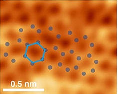
Image Caption: Graphene, a super tough wonder material, hasn’t made it into electronics yet because it doesn’t conduct an electric current on its own. Researchers used a laser technique to permanently stress graphene into a structure that allows the flow of electric current. (Purdue University image/Gary Cheng)
This structure is a so-called “band gap.” Electrons need to jump across this gap in order to become conduction electrons, which makes them capable of carrying electric current. But graphene doesn’t naturally have a band gap.
Purdue researchers created and widened the band gap in graphene to a record 2.1 electronvolts. To function as a semiconductor such as silicon, the band gap would need to be at least the previous record of 0.5 electronvolts.
“This is the first time that an effort has achieved such high band gaps without affecting graphene itself, such as through chemical doping. We have purely strained the material,” said Gary Cheng, professor of industrial engineering at Purdue, whose lab has investigated various ways to make graphene more useful for commercial applications.
The presence of a band gap allows semiconductor materials to switch between insulating or conducting an electric current, depending on whether their electrons are pushed across the band gap or not.
Surpassing 0.5 electronvolts unlocks even more potential for graphene in next-generation electronic devices, the researchers say. Their work appears in an issue of Advanced Materials.
“Researchers in the past opened the band gap by simply stretching graphene, but stretching alone doesn’t widen the band gap very much. You need to permanently change the shape of graphene to keep the band gap open,” Cheng said.
Cheng and his collaborators not only kept the band gap open in graphene, but also made it to where the gap width could be tuned from zero to 2.1 electronvolts, giving scientists and manufacturers the option to just use certain properties of graphene depending on what they want the material to do.
The researchers made the band gap structure permanent in graphene using a technique called laser shock imprinting, which Cheng developed in 2014 along with scientists at Harvard University, the Madrid Institute for Advanced Studies and the University of California, San Diego.
For this study, the researchers used a laser to create shockwave impulses that penetrated an underlying sheet of graphene. The laser shock strains graphene onto a trench-like mold – permanently shaping it. Adjusting the laser power adjusts the band gap.
While still far from putting graphene into semiconducting devices, the technique grants more flexibility in taking advantage of the material’s optical, magnetic and thermal properties, Cheng said.
The work was supported by multiple entities, including the National Science Foundation (Grant numbers CMMI-0547636 and CMMI 0928752) and the National Research Council Senior Research Associateship.
Share on:


Suggested Items
Zentech’s Board of Directors Announces the Return of Matt Turpin as President and CEO
04/22/2024 | Zentech ManufacturingTurpin draws upon over 35 years of experience in the electronics industry and has an 18-year history with Zentech. He previously served as President and CEO from 2006 to 2019 after which time he has remained active in the EMS industry as an advisor to Zentech and other industry organizations.
SEMI Talent Forum 2024 to Help Build Next-Generation Chip Industry Workforce
04/09/2024 | SEMIPost-graduates and onboarding talent will connect with local companies to explore semiconductor industry career paths and employment opportunities at the SEMI Talent Forum, May 1, 2024 at the University of Swansea.
Indium Corporation Technical Manager to Present at SMTA Taiwan Tech Forum
03/12/2024 | Indium CorporationIndium Corporation Senior Area Technical Manager Jason Chou will present at the SMTA Taiwan Tech Forum on March 26 in Taoyuan City, Taiwan. Chou’s presentation will highlight the growing demand for high reliability and low-temperature solder solutions brought on by the rapidly developing electric vehicle (EV) and artificial intelligence (AI) industries.
Fujitsu, Delft University of Technology Establish New Quantum Lab
01/26/2024 | JCN NewswireFujitsu and Delft University of Technology today announced the establishment of the Fujitsu Advanced Computing Lab Delft at Delft University of Technology, an industry-academia collaboration hub dedicated to the development of quantum computing technologies.
Foundations of the Future: Awarding Scholarships and Awards in 2023
01/24/2024 | IPC Education Foundation -- Column: Foundations of the FutureProviding scholarships and awards to hard-working students who excel academically, demonstrate a commitment to electronics manufacturing, and are active members of the IPC student network, supports the overall mission of the IPC Education Foundation, which is to develop a talent pipeline for the industry.