


 It’s Only Common Sense: OCCAM—the Time Is Now
 Marcy's Musings: The Growing Industry
 Dan’s Biz Bookshelf: Seeing the How
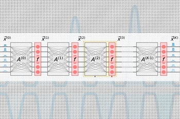
MIT researchers have developed a novel “photonic” chip that uses light instead of electricity — and consumes relatively little power in the process. The chip could be used to process massive neural networks millions of times more efficiently than today’s classical computers do.
Image Caption: A new photonic chip design drastically reduces energy needed to compute with light, with simulations suggesting it could run optical neural networks 10 million times more efficiently than its electrical counterparts.
Neural networks are machine-learning models that are widely used for such tasks as robotic object identification, natural language processing, drug development, medical imaging, and powering driverless cars. Novel optical neural networks, which use optical phenomena to accelerate computation, can run much faster and more efficiently than their electrical counterparts.
But as traditional and optical neural networks grow more complex, they eat up tons of power. To tackle that issue, researchers and major tech companies — including Google, IBM, and Tesla — have developed “AI accelerators,” specialized chips that improve the speed and efficiency of training and testing neural networks.
For electrical chips, including most AI accelerators, there is a theoretical minimum limit for energy consumption. Recently, MIT researchers have started developing photonic accelerators for optical neural networks. These chips perform orders of magnitude more efficiently, but they rely on some bulky optical components that limit their use to relatively small neural networks.
In a paper published in Physical Review X, MIT researchers describe a new photonic accelerator that uses more compact optical components and optical signal-processing techniques, to drastically reduce both power consumption and chip area. That allows the chip to scale to neural networks several orders of magnitude larger than its counterparts.
Simulated training of neural networks on the MNIST image-classification dataset suggest the accelerator can theoretically process neural networks more than 10 million times below the energy-consumption limit of traditional electrical-based accelerators and about 1,000 times below the limit of photonic accelerators. The researchers are now working on a prototype chip to experimentally prove the results.
“People are looking for technology that can compute beyond the fundamental limits of energy consumption,” says Ryan Hamerly, a postdoc in the Research Laboratory of Electronics. “Photonic accelerators are promising … but our motivation is to build a [photonic accelerator] that can scale up to large neural networks.”
Practical applications for such technologies include reducing energy consumption in data centers. “There’s a growing demand for data centers for running large neural networks, and it’s becoming increasingly computationally intractable as the demand grows,” says co-author Alexander Sludds, a graduate student in the Research Laboratory of Electronics. The aim is “to meet computational demand with neural network hardware … to address the bottleneck of energy consumption and latency.”
Joining Sludds and Hamerly on the paper are: co-author Liane Bernstein, an RLE graduate student; Marin Soljacic, an MIT professor of physics; and Dirk Englund, an MIT associate professor of electrical engineering and computer science, a researcher in RLE, and head of the Quantum Photonics Laboratory.
Page 1 of 2
Share on:


Suggested Items
KIC’s Miles Moreau to Present Profiling Basics and Best Practices at SMTA Wisconsin Chapter PCBA Profile Workshop
01/25/2024 | KICKIC, a renowned pioneer in thermal process and temperature measurement solutions for electronics manufacturing, announces that Miles Moreau, General Manager, will be a featured speaker at the SMTA Wisconsin Chapter In-Person PCBA Profile Workshop.
The Drive Toward UHDI and Substrates
09/20/2023 | I-Connect007 Editorial TeamPanasonic’s Darren Hitchcock spoke with the I-Connect007 Editorial Team on the complexities of moving toward ultra HDI manufacturing. As we learn in this conversation, the number of shifting constraints relative to traditional PCB fabrication is quite large and can sometimes conflict with each other.
Standard Of Excellence: The Products of the Future
09/19/2023 | Anaya Vardya -- Column: Standard of ExcellenceIn my last column, I discussed cutting-edge innovations in printed circuit board technology, focusing on innovative trends in ultra HDI, embedded passives and components, green PCBs, and advanced substrate materials. This month, I’m following up with the products these new PCB technologies are destined for. Why do we need all these new technologies?
Experience ViTrox's State-of-the-Art Offerings at SMTA Guadalajara 2023 Presented by Sales Channel Partner—SMTo Engineering
09/18/2023 | ViTroxViTrox, which aims to be the world’s most trusted technology company, is excited to announce that our trusted Sales Channel Partner (SCP) in Mexico, SMTo Engineering, S.A. de C.V., will be participating in SMTA Guadalajara Expo & Tech Forum. They will be exhibiting in Booth #911 from the 25th to the 26th of October 2023, at the Expo Guadalajara in Jalisco, Mexico.
Intel Unveils Industry-Leading Glass Substrates to Meet Demand for More Powerful Compute
09/18/2023 | IntelIntel announced one of the industry’s first glass substrates for next-generation advanced packaging, planned for the latter part of this decade.