


 It’s Only Common Sense: OCCAM—the Time Is Now
 Marcy's Musings: The Growing Industry
 Dan’s Biz Bookshelf: Seeing the How
Researchers ‘Stretch’ the Ability of 2D Materials to Change Technology
June 12, 2019 | University of RochesterEstimated reading time: 5 minutes
Two-dimensional (2D) materials—as thin as a single layer of atoms—have intrigued scientists with their flexibility, elasticity, and unique electronic properties since first being discovered in materials such as graphene in 2004. Some of these materials can be especially susceptible to changes in their material properties as they are stretched and pulled. Under applied strain, they have been predicted to undergo phase transitions as disparate as superconducting in one moment to nonconducting the next, or optically opaque in one moment to transparent in the next.
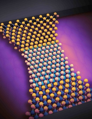
Image Caption: Artist’s rendering of a 2D material undergoing phase change using a transistor-scale platform developed in the lab of Stephen Wu, assistant professor of electrical and computer engineering and of physics. (University of Rochester illustration / Michael Osadciw)
Now, University of Rochester researchers have combined 2D materials with oxide materials in a new way, using a transistor-scale device platform, to fully explore the capabilities of these changeable 2D materials to transform electronics, optics, computing, and a host of other technologies.
“We’re opening up a new direction of study,” says Stephen Wu, assistant professor of electrical and computer engineering and physics. “There’s a huge number of 2D materials with different properties—and if you stretch them, they will do all sorts of things.”
The platform developed in Wu’s lab, configured much like traditional transistors, allows a small flake of a 2D material to be deposited onto a ferroelectric material. Voltage applied to the ferroelectric—which acts like a transistor’s third terminal, or gate—strains the 2D material by the piezoelectric effect, causing it to stretch. That, in turn, triggers a phase change that can completely alter the way the material behaves. When the voltage is turned off, the material retains its phase until an opposite polarity voltage is applied, causing the material to revert to its original phase.
“The ultimate goal of two-dimensional straintronics is to take all of the things that you couldn’t control before, like the topological, superconducting, magnetic, and optical properties of these materials, and now be able to control them, just by stretching the material on a chip,” Wu says.
“If you do this with topological materials you could impact quantum computers, or if you do it with superconducting materials you can impact superconducting electronics.”
Maxing out Moore’s Law
In a paper in Nature Nanotechnology, Wu and his students describe using a thin film of two-dimensional molybdenum ditelluride (MoTe2) in the device platform. When stretched and unstretched, the MoTe2 changes from a low conductivity semiconductor material to a highly conductive semimetallic material and back again.
“It operates just like a field effect transistor. You just have to put a voltage on that third terminal, and the MoTe2 will stretch a little bit in one direction and become something that’s conducting. Then you stretch it back in another direction, and all of a sudden you have something that has low conductivity,” Wu says.
The process works at room temperature, he adds, and, remarkably, “requires only a small amount of strain—we’re stretching the MoTe2 by only 0.4 percent to see these changes.”
Moore’s Law famously predicts that the number of transistors in a dense, integrated circuit will double about every two years.
Yet technology is nearing the limits at which traditional transistors can be scaled down in size. So, as we reach the limits of Moore’s Law, the technology developed in Wu’s lab could have far-reaching implications in moving past these limitations in the quest for ever faster, more enhanced computing power.
Wu’s platform has the potential to perform the same functions as a transistor with far less power consumption since power is not needed to retain the conductivity state. Moreover, it minimizes the leakage of electrical current due to the steep slope at which the device changes conductivity with applied gate voltage. Both of these issues—high power consumption and leakage of electrical current—have constrained the performance of traditional transistors at the nanoscale.
“This is the first demonstration,” Wu adds. “Now it’s up to researchers to figure out how far it goes.”
No Strain, No Gain
One advantage of Wu’s platform is that it is configured much like a traditional transistor, making it easier to eventually adapt into current electronics. However, more work is needed before the platform reaches that stage. Currently, the device can operate only 70 to 100 times in the lab before device failure. While the endurance of other non-volatile memories, like flash, are much higher, they also operate much slower than the ultimate potential of the strain-based devices being developed in Wu’s lab.
“Do I think it’s a challenge that can be overcome? Absolutely,” says Wu, who will be working on the problem with Hesam Askari, an assistant professor of mechanical engineering at Rochester, also a coauthor on the paper. “It’s a materials engineering problem that we can solve as we move forward in our understanding how this concept works.”
They will also explore how much strain can be applied to various two-dimensional materials without causing them to break. Determining the ultimate limit of the concept will help guide researchers to other phase-change materials as the technology moves forward.
Wu, who completed his PhD in physics at the University of California, Berkeley, was a postdoctoral scholar in the Materials Science Division at Argonne National Laboratory before he joined the University of Rochester as an assistant professor in the Department of Electrical and Computer Engineering and the Department of Physics and Astronomy in 2017.
He started with a single undergraduate student in his lab—Arfan Sewaket ’19, who was spending the summer as a Xerox Research Fellow. She helped Wu set up a temporary lab, then was the first to try out the device concept and the first to demonstrate its feasibility. Since then, four graduate students in Wu’s lab—lead author Wenhui Hou, Ahmad Azizimanesh, Tara Peña, and Carla Watson—“have done so much work” to document the device’s properties and refine it, creating about 200 different versions to this point, Wu says. All are listed with Sewaket as coauthors, along with Askari and Ming Liu of Xi’an Jiaotong University in China.
Share on:


Suggested Items
Groundbreaking Ceremony Marks the Beginning of a New Era for Newccess Industrial; The Construction of the MINGXIN Building
04/12/2024 | Newccess IndustrialOn a clear and sunny day in March, the groundbreaking ceremony for the MINGXIN Building took place in Shenzhen, China. This moment marked the official commencement of construction for a project that will reshape the semiconductor materials industry.
The Need for a Holistic Global Sustainability Standard
04/10/2024 | Michael Ford, Aegis SoftwareNo one can deny that the resources of our fragile planet are finite. The environment seems like a third party, subject to constant degradation. We’re acutely aware of the effects of pollution on our climate, and despite our “throw-away” culture, recycling and recovery of materials has remained relatively expensive, even as we use more energy just to survive.
iNEMI Publishes Four Roadmap Topics
04/04/2024 | iNEMIThe International Electronics Manufacturing Initiative (iNEMI) announces the availability of the first roadmap topics in the new iNEMI Roadmap format. Printed circuit boards, sustainable electronics, smart manufacturing, and mmWave materials and test are now available online.
Insulectro’s 'Storekeepers' Extend Their Welcome to Technology Village at IPC APEX EXPO
04/03/2024 | InsulectroInsulectro, the largest distributor of materials for use in the manufacture of PCBs and printed electronics, welcomes attendees to its TECHNOLOGY VILLAGE during this year’s IPC APEX EXPO at the Anaheim Convention Center, April 9-11, 2024.
Checking In With ICAPE Group
04/03/2024 | Nolan Johnson, I-Connect007ICAPE Group’s field application engineer Erik Pederson drills down on sustainability, supply chain resiliency, and what value engineering really looks like in this exclusive interview. Founded in 1999, European-based ICAPE Group provides 21 million printed circuit boards and over six million technical parts to manufacturers every month. With 30 PCB manufacturing partners globally and 50 partners providing a wide array of technical parts, ICAPE Group has operations in China, Taiwan, Thailand, South Korea, Vietnam, South Africa, Europe, Mexico, and the United States. The company also focuses on the value proposition for its customers.