


 The Right Approach: I Hear the Train A Comin'
 It’s Only Common Sense: OCCAM—the Time Is Now
 Marcy's Musings: The Growing Industry
Tune in to Future Polarity Quantum Devices
June 13, 2019 | ICN2Estimated reading time: 2 minutes
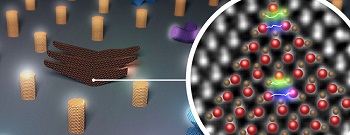
A thorough study published in NanoLetters and led by the ICN2 Advanced Electron Nanoscopy group provides new insights on the growth mechanisms and conditions that determine the polarity of semiconductor nanostructures. Fine control of polarity can result in the design of new quantum devices.
Future applications of nanomaterials depend on our ability to understand their characteristics at the atomic scale and to modulate them at will. Polarity appears to play an important role in determining the physical and morphological properties of semiconductor nanostructures, thus researchers are studying how to control or change it.
Because of the way atoms are arranged in crystal structures, electromagnetic charges are locally separated. As a consequence, if we look at the crystal along specific directions, we can observe oppositely-charged ionic couples, which are called dumbbells because of their shape. Binary compounds—i.e. formed by two elements only—are said to have A- or B- polarity according to the dumbbell orientation. The type of polarity of these materials influences their properties, which, in turn, have a remarkable impact on the final applications.
An extensive study on polarity of semiconductor materials, conducted by Dr. María de la Mata, ICREA Prof. Jordi Arbiol and Sara Martí-Sánchez from the ICN2 Advanced Electron Nanoscopy group, in collaboration with researchers at the École Polytechnique Fédérale of Lausanne (Switzerland), the University of Bremen (Germany), the Nanyang Technological University (Singapore) and the Microsoft Quantum Lab of Delft (The Netherlands), has been recently published on NanoLetters.
Nanostructures of a wide range of semiconductor compounds have been grown in laboratory and then analyzed, using scanning transmission electron microscopy, in order to determine their polarity and compile a complete mapping. The researchers have observed that most of these materials spontaneously grow along the B-polar direction, while only a few follow either A- or B- polar directions. The latter are particularly interesting, as potentially they could offer us the possibility to predetermine their polarity during growth by intervening on some variables.
The aim of this study was indeed to pin down the factors that influence the polarity of non-planar nanostructures. Since, from the analysis of the new results and previously reported data, did not emerge any parameter that would relate the type of polarity with a specific family of binary compounds, it was concluded that the observed polarity of these nanostructures is strictly connected to the growth conditions and techniques.
Experiments have been carried out using both particle-assisted and non-particle-assisted growth techniques, which differ in the structure development starting from a core of solid material or not, and varying other parameters. Even though a complete comprehension of the dynamic and kinetics of the growing process has not been achieved yet, this study moves forward our knowledge of the mechanisms determining the growth polarity at the nanoscale. It also provides an overview of the parameters that can be tuned during the growth to influence the polarity of the resulting nanostructure. Once a fine control capability is reached, it will be possible to engineer new structures with preselected or changeable polarity with the aim to develop novel quantum devices.
Share on:


Suggested Items
Real Time with... IPC APEX EXPO 2024: Sustainability in the Industry
04/26/2024 | Real Time with...IPC APEX EXPOGuest Editor Henry Crandall and Chris Nash of Indium Corporation discuss the company's 90th anniversary and its focus on sustainability. They focus on the benefits of sustainable materials, their compatibility, and value propositions. The conversation also highlights how Durafuse LT technology's role in reducing reflow temperatures is leading to significant cost and energy savings. Nash also touches on downstream sustainability efforts such as using recycled materials for packaging.
SMC Korea 2024 to Highlight Semiconductor Materials Trends and Innovations on Industry’s Path to $1 Trillion
04/24/2024 | SEMIWith Korea a major consumer of semiconductor materials and advanced materials a key driver of innovation on the industry’s path to $1 trillion, industry leaders and experts will gather at SMC (Strategic Materials Conference) Korea 2024 on May 29 at the Suwon Convention Center in Gyeonggi-do, South Korea to provide insights into the latest materials developments and trends. Registration is open.
Groundbreaking Ceremony Marks the Beginning of a New Era for Newccess Industrial; The Construction of the MINGXIN Building
04/12/2024 | Newccess IndustrialOn a clear and sunny day in March, the groundbreaking ceremony for the MINGXIN Building took place in Shenzhen, China. This moment marked the official commencement of construction for a project that will reshape the semiconductor materials industry.
The Need for a Holistic Global Sustainability Standard
04/10/2024 | Michael Ford, Aegis SoftwareNo one can deny that the resources of our fragile planet are finite. The environment seems like a third party, subject to constant degradation. We’re acutely aware of the effects of pollution on our climate, and despite our “throw-away” culture, recycling and recovery of materials has remained relatively expensive, even as we use more energy just to survive.
iNEMI Publishes Four Roadmap Topics
04/04/2024 | iNEMIThe International Electronics Manufacturing Initiative (iNEMI) announces the availability of the first roadmap topics in the new iNEMI Roadmap format. Printed circuit boards, sustainable electronics, smart manufacturing, and mmWave materials and test are now available online.