


 Marcy's Musings: The Growing Industry
 It’s Only Common Sense: Here’s What To Do After IPC APEX EXPO 2024
 Dan’s Biz Bookshelf: Seeing the How
Photovoltaic Nanotubes
June 20, 2019 | University of TokyoEstimated reading time: 3 minutes
Physicists discovered a novel kind of nanotube that generates current in the presence of light. Devices such as optical sensors and infrared imaging chips are likely applications, which could be useful in fields such as automated transport and astronomy. In future, if the effect can be magnified and the technology scaled up, it could lead to high-efficiency solar power devices.
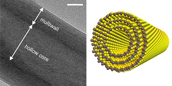
Image Caption: Transmission electron microscopy image of a hollow core nanotube. The white scale bar corresponds to 10 nanometers (left). Rendering of a nanotube (right).
Working with an international team of physicists, University of Tokyo Professor Yoshihiro Iwasa was exploring possible functions of a special semiconductor nanotube when he had a lightbulb moment. He took this proverbial lightbulb (which was in reality a laser) and shone it on the nanotube to discover something enlightening. Certain wavelengths and intensities of light induced a current in the sample — this is called the photovoltaic effect. There are several photovoltaic materials, but the nature and behavior of this nanotube is cause for excitement.
“Essentially our research material generates electricity like solar panels, but in a different way,” said Iwasa. “Together with Dr. Yijin Zhang from the Max Planck Institute for Solid State Research in Germany, we demonstrated for the first time nanomaterials could overcome an obstacle that will soon limit current solar technology. For now solar panels are as good as they can be, but our technology could improve upon that.”
The current-inducing nanotube is made from rolled-up sheets of a special semiconductor material based on tungsten disulfide (WS2). The sheets do not induce a current in the presence of light unless rolled into tubes. This is an emergent behavior, one not intrinsic to the material until it’s modified. What is interesting is how it differs from existing photovoltaic materials.
Generally, photovoltaic solar panels make use of a certain arrangement of materials called a p-n junction. This is where two different kinds of materials (p-type and n-type) are attached, which alone do not generate a current in the presence of light, but when placed together, do. P-n junction-based photovoltaics have improved in efficiency over the 80 years or so since their discovery. However, they are getting close to their theoretical limits due in part to their need for the arrangement of multiple materials.
WS2 nanotubes do not rely on a junction between materials to gain the photovoltaic effect. When exposed to light, they generate a current throughout their entire structure or bulk. This is called the bulk photovoltaic effect (BPVE) and it occurs as the WS2 nanotube is not symmetrical if you were to reverse it. If it were symmetrical, the current induced would not have a preferred direction and thus would not flow. So other symmetrical nanotubes — such as the famous carbon nanotubes — don't exhibit BPVE despite being great electrical conductors.
Four inset images. The lower right is a coarse grey texture. The other othree are orange geometric shapes on dark backgrounds.
Image Caption: Various iterations of the experimental nanotube device. Images captured by an atomic force microscope, and a scanning Kelvin probe microscope (lower right).
“Our research shows an entire order of magnitude improvement in efficiency of BPVE compared to its presence in other materials,” continued Iwasa. “But despite this huge gain, our WS2 nanotube cannot yet compare to the generating potential of p-n junction materials. This is because the device is nanoscopic and will be difficult to make larger. But it is possible and I hope chemists are inspired to take on that challenge.”
In the long term, researchers hope this kind of material could allow fabrication of more efficient solar panels. But given the foreseeable size constraints in the near term, it’s more likely to find use in other applications. BVPE could be used to create more sensitive and higher-fidelity optical or infrared sensors. These have further applications in embedded monitoring devices, sensor-laden self-driving cars or even in the imaging sensors for astronomical telescopes.
“My colleagues from around the world and I eagerly explore the potential of this unprecedented technology,” concluded Iwasa. “For me, the idea of creating new materials beyond anything nature could provide is a fascinating reward in its own right.”
Share on:


Suggested Items
Australian Flow Batteries and The SCHMID Group Announce Groundbreaking Memorandum of Understanding
04/17/2024 | SCHMID GroupAustralian Flow Batteries Pty Ltd (AFB), a leader in innovative energy solutions and economical, safe, and reliable power storage, and SCHMID Energy Systems GmbH a company of the German SCHMID Group, a global technology leader with a rich history in delivering innovative solutions across multiple industries including Electronics, Renewables, and Energy Storage sectors, are thrilled to announce the signing of a Memorandum of Understanding (MoU)
Ansys Joins BAE Systems’ Mission Advantage Program to Advance Digital Engineering Across US Department of Defense
04/16/2024 | ANSYSAnsys announced it is working with BAE Systems, Inc., to accelerate the adoption of digital engineering and MBSE across the Department of Defense (DoD).
Microchip Technology Acquires Neuronix AI Labs
04/16/2024 | Microchip Technology Inc.Innovative technology enhances AI-enabled intelligent edge solutions and increases neural networking capabilities.
Incap Estonia Teamed Up With Solaride to Fuel Youth Excitement for The World of Engineering
04/11/2024 | IncapIncap Estonia partnered with Solaride to ignite enthusiasm among young people for the world of engineering and sustainable technology. Together, they organised an inspiring day for students from grades 7 through 12 in Saaremaa. Held at Incap’s Kuressaare factory, this event brought together over 130 young minds eager to explore the innovative world of technology and learn more about advanced electronics manufacturing.
Plastronics and the New IPC Guidelines for In-mold Electronics (IME)
04/11/2024 | Barry Matties, I-Connect007In the ever-evolving world of electronics, the roads for the integration of electronics assemblies into 3D structures continue to grow into a set of technologies used to produce 3D plastronics parts and revolutionize mainly the automotive industry. IPC has been developing standards for this set of technologies, led by Francisco Fourcade, IPC electronics technology standards manager.