


 It’s Only Common Sense: OCCAM—the Time Is Now
 Marcy's Musings: The Growing Industry
 Dan’s Biz Bookshelf: Seeing the How
Researchers Explain Visible Light from 2D Lead Halide Perovskites
June 26, 2019 | University of HoustonEstimated reading time: 2 minutes
Researchers drew attention three years ago when they reported that a two-dimensional perovskite—a material with a specific crystal structure—composed of cesium, lead and bromine emitted a strong green light.
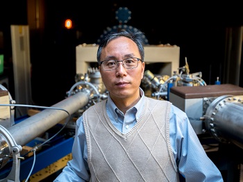
Image Caption: Jiming Bao, associate professor of electrical and computer engineering, led an international group of researchers investigating how a two-dimensional perovskite composed of cesium, lead and bromine was able to emit a strong green light.
Crystals that produce light on the green spectrum are desirable because green light, while valuable in itself, can also be relatively easily converted to other forms that emit blue or red light, making it especially important for optical applications ranging from light-emitting devices to sensitive diagnostic tools.
But there was no agreement about how the crystal, CsPB2Br5, produced the green photoluminescence. Several theories emerged, without a definitive answer.
Now, however, researchers from the United States, Mexico and China, led by an electrical engineer from the University of Houston, have reported in the journal Advanced Materials they have used sophisticated optical and high-pressure diamond anvil cell techniques to determine not only the mechanism for the light emission but also how to replicate it.
They initially synthesized CsPB2Br5 from a related material known as CsPbBr3 and found that the root cause of the light emission is a small overgrowth of nanocrystals composed of that original material, growing along the edge of the CsPB2Br5 crystals. While CsPbBr3, the base crystal, is three-dimensional and appears green under ultraviolet light, the new material, CsPB2Br5, has a layered structure and is optically inactive.
“Now that the mechanism for emitting this light is understood, it can be replicated,” said Jiming Bao, associate professor of electrical and computer engineering at UH and corresponding author on the paper. “Both crystals have the same chemical composition, much like diamond versus graphite, but they have very different optical and electronic properties. People will be able to integrate the two materials to make better devices.”
Potential applications range from solar cells to LED lighting and other electronic devices.
Bao began working on the problem in 2016, a project that ultimately involved 19 researchers from UH and institutions in China and Mexico. At the time, there were two schools of scientific thought on the light emission from the cesium crystal: that it emitted green light due to a defect, mainly a lack of bromine, rather than the material itself, or that a variation had unintentionally been introduced, resulting in the emission.
His group started with the synthesis of a clean sample by dropping CsPbBr3 powder in water, resulting in sharper-edged crystals. The sharper edges emitted a stronger green light, Bao said.
The researchers then used an optical microscope to study the individual crystals of the compound, which Bao said allowed them to determine that although the compound is transparent, “something was going on at the edge, resulting in the photoluminescence.”
They relied on Raman spectroscopy—an optical technique that uses information about how light interacts with a material to determine the material’s lattice properties—to identify nanocrystals of the original source material, CsPbBr3, along the edges of the crystal as the source of the light.
Bao said CsPbBr3 is too unstable to use on its own, but the stability of the converted form isn’t hampered by the small amount of the original crystal.
The researchers said the new understanding of the light emission will yield new opportunities to design and fabricate novel optoelectronic devices. The techniques used to understand the cesium-lead-halide compound can also be applied to other optical materials to learn more about how they emit light, Bao said.
Share on:


Suggested Items
Groundbreaking Ceremony Marks the Beginning of a New Era for Newccess Industrial; The Construction of the MINGXIN Building
04/12/2024 | Newccess IndustrialOn a clear and sunny day in March, the groundbreaking ceremony for the MINGXIN Building took place in Shenzhen, China. This moment marked the official commencement of construction for a project that will reshape the semiconductor materials industry.
The Need for a Holistic Global Sustainability Standard
04/10/2024 | Michael Ford, Aegis SoftwareNo one can deny that the resources of our fragile planet are finite. The environment seems like a third party, subject to constant degradation. We’re acutely aware of the effects of pollution on our climate, and despite our “throw-away” culture, recycling and recovery of materials has remained relatively expensive, even as we use more energy just to survive.
Altus Group Celebrates 30 Years of Innovation with Scienscope
04/08/2024 | Altus GroupAltus Group, a prominent distributor of capital equipment within the electronics industry across the UK and Ireland, is pleased to commemorate the 30th anniversary of Scienscope International, a leading supplier of advanced inspection solutions.
iNEMI Publishes Four Roadmap Topics
04/04/2024 | iNEMIThe International Electronics Manufacturing Initiative (iNEMI) announces the availability of the first roadmap topics in the new iNEMI Roadmap format. Printed circuit boards, sustainable electronics, smart manufacturing, and mmWave materials and test are now available online.
Insulectro’s 'Storekeepers' Extend Their Welcome to Technology Village at IPC APEX EXPO
04/03/2024 | InsulectroInsulectro, the largest distributor of materials for use in the manufacture of PCBs and printed electronics, welcomes attendees to its TECHNOLOGY VILLAGE during this year’s IPC APEX EXPO at the Anaheim Convention Center, April 9-11, 2024.