


 Marcy's Musings: The Growing Industry
 It’s Only Common Sense: Here’s What To Do After IPC APEX EXPO 2024
 Dan’s Biz Bookshelf: Seeing the How
Search for New Semiconductors Heats up With Gallium Oxide
July 23, 2019 | University of IllinoisEstimated reading time: 2 minutes
University of Illinois electrical engineers have cleared another hurdle in high-power semiconductor fabrication by adding the field’s hottest material—beta-gallium oxide—to their arsenal. Beta-gallium oxide is readily available and promises to convert power faster and more efficiently than today’s leading semiconductor materials—gallium nitride and silicon, the researchers said.
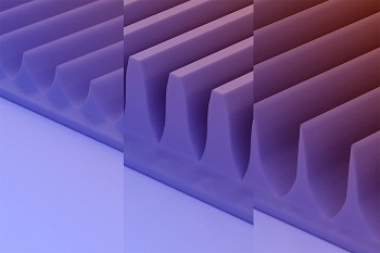
Flat transistors have become about as small as is physically possible, but researchers addressed this problem by going vertical. With a technique called metal-assisted chemical etching—or MacEtch—U. of I. engineers used a chemical solution to etch semiconductor into 3D fin structures. The fins increase the surface area on a chip, allowing for more transistors or current, and can therefore handle more power while keeping the chip’s footprint the same size.
Developed at the U. of I., the MacEtch method is superior to traditional “dry” etching techniques because it is far less damaging to delicate semiconductor surfaces, such as beta-gallium oxide, researchers said.
“Gallium oxide has a wider energy gap in which electrons can move freely,” said the study’s lead author Xiuling Li, a professor of electrical and computer engineering. “This energy gap needs to be large for electronics with higher voltages and even low-voltage ones with fast switching frequencies, so we are very interested in this type of material for use in modern devices. However, it has a more complex crystal structure than pure silicon, making it difficult to control during the etching process.”
Applying MacEtch to gallium oxide crystals could benefit the semiconductor industry, Li said, but the advancement is not without hurdles.
“Right now, the etching process is very slow,” she said. “Because of the slow rate and the complex crystal structure of the material, the 3D fins produced are not perfectly vertical, and vertical fins are ideal for efficient use of power.”
In the new study, the beta-gallium oxide substrate produced triangular, trapezoidal and tapered fins, depending on the orientation of metal catalyst layout relative to the crystals. Although these shapes are not ideal, the researchers were surprised to find that they still do a better job conducting current than the flat, unetched beta-gallium oxide surfaces.
“We are not sure why this is the case, but we are starting to get some clues by performing atomic-level characterizations of the material,” Li said. “The bottom line is that we have shown it is possible to use the MacEtch process to fabricate beta-gallium oxide, a potentially low-cost alternative to gallium nitride, with good interface quality.”
Li said further research will need to address the slow etch rate, enable high performance beta-gallium oxide devices, and try to get around the problem of low thermal conductivity.
“Increasing the etch rate should improve the process’s ability to form more vertical fins,” she said. “This is because the process will happen so quickly that it will not have time to react to all of the differences in crystal orientations.”
The low thermal conductivity issue is a deeper problem, she said. “High-power electronics produce a lot of heat, and device researchers are actively seeking thermal engineering solutions. While this is a wide-open aspect in the semiconductor field right now, 3D structures like what we have demonstrated could help guide the heat out better in some device types.”
Li is affiliated with the Nick Holonyak Jr. Micro and Nanotechnology Laboratory, the Frederick Seitz Materials Research Laboratory and the Beckman Institute for Advanced Science and Technology at the U. of I.
The National Science Foundation and the U.S. Department of Energy supported this research.
Share on:


Suggested Items
KIC’s Miles Moreau to Present Profiling Basics and Best Practices at SMTA Wisconsin Chapter PCBA Profile Workshop
01/25/2024 | KICKIC, a renowned pioneer in thermal process and temperature measurement solutions for electronics manufacturing, announces that Miles Moreau, General Manager, will be a featured speaker at the SMTA Wisconsin Chapter In-Person PCBA Profile Workshop.
The Drive Toward UHDI and Substrates
09/20/2023 | I-Connect007 Editorial TeamPanasonic’s Darren Hitchcock spoke with the I-Connect007 Editorial Team on the complexities of moving toward ultra HDI manufacturing. As we learn in this conversation, the number of shifting constraints relative to traditional PCB fabrication is quite large and can sometimes conflict with each other.
Standard Of Excellence: The Products of the Future
09/19/2023 | Anaya Vardya -- Column: Standard of ExcellenceIn my last column, I discussed cutting-edge innovations in printed circuit board technology, focusing on innovative trends in ultra HDI, embedded passives and components, green PCBs, and advanced substrate materials. This month, I’m following up with the products these new PCB technologies are destined for. Why do we need all these new technologies?
Experience ViTrox's State-of-the-Art Offerings at SMTA Guadalajara 2023 Presented by Sales Channel Partner—SMTo Engineering
09/18/2023 | ViTroxViTrox, which aims to be the world’s most trusted technology company, is excited to announce that our trusted Sales Channel Partner (SCP) in Mexico, SMTo Engineering, S.A. de C.V., will be participating in SMTA Guadalajara Expo & Tech Forum. They will be exhibiting in Booth #911 from the 25th to the 26th of October 2023, at the Expo Guadalajara in Jalisco, Mexico.
Intel Unveils Industry-Leading Glass Substrates to Meet Demand for More Powerful Compute
09/18/2023 | IntelIntel announced one of the industry’s first glass substrates for next-generation advanced packaging, planned for the latter part of this decade.