


 It’s Only Common Sense: OCCAM—the Time Is Now
 Marcy's Musings: The Growing Industry
 Dan’s Biz Bookshelf: Seeing the How
Development of Simplified New Mass Spectrometric Technique using Laser and Graphene
August 13, 2019 | DGISTEstimated reading time: 2 minutes
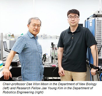
A technology that can obtain high-resolution, micrometer-sized images for mass spectrometric analysis without sample preparation has been developed. DGIST Research Fellow Jae Young Kim and Chair-professor Dae Won Moon’s team succeeded in developing the precise analysis and micrometer-sized imaging of bio samples using a small and inexpensive laser.
DGIST announced that Research Fellow Jae Young Kim in the Department of Robotics Engineering and Chair-professor Dae Won Moon’s team developed a technology that can analyze experiment samples without any preparation processing. Due to its ability to obtain high-resolution mass spectrometric images without an experimental environment using ‘continuous wave laser, the technology is expected to be applied widely in the precise medicine and medical diagnosis fields.
Many advance preparations are needed for the mass spectrometric imaging of biometric samples using ‘specimen,’ which thinly cut an object to analyze. The specimen must be changed artificially since they cannot be analyzed accurately in a room temperature or atmospheric pressure. To develop a convenient analysis technology and ease the burden, Research Fellow Kim started the research.
The research team installed a lens carrying continuous wave laser right below a microscope substrate where the specimen is put and shot the laser on it to measure mass spectra by examining molecules from desorption.
The mass spectra can be analyzed through a continuous wave laser whose energy is weaker than other lasers because of the use of ‘graphene substrate’ below the specimen.
Since the honeycomb-patterned graphene has very high heat conductivity and can convert light into heat, it can secure enough heat needed for specimen analysis with small amount of light generated by the continuous wave laser. This technology is also advantageous for obtaining high-resolution analysis images, because it can secure space to observe specimen much more closely even when using a 20x magnifying lens.
Chair-professor Dae Won Moon in the Department of New Biology explained that “Through this technology, we could greatly shorten the preparation time for analysis by omitting the specimen preprocessing step. Our next plan is to develop the technology further so it can be applied in various areas such as medical diagnosis.”
This research was participated by Research Fellow Jae Young Kim in the Department of Robotics Engineering and Ph.D. candidate Heejin Lim in the Department of New Biology as the co-first authors and was conducted with Professor Cheol Song in the Department of Robotics Engineering at DGIST, Professor Dong-Kwon Lim at Korea University, and Research Professor Ji-Won Park at Chungnam National University.
Share on:


Suggested Items
Koh Young Showcases Award-winning Inspection Solutions at SMTconnect with SmartRep in Hall 4A.225
04/25/2024 | Koh Young TechnologyKoh Young Technology, the industry leader in True 3D measurement-based inspection solutions, will showcase an array of award-winning inspection and measurement solutions at SMTconnect alongside its sales partner, SmartRep, in booth 4A.225 at NürnbergMesse from June 11-13, 2023. The following offers a glimpse into what Koh Young will present at the tradeshow:
Real Time with… IPC APEX EXPO 2024: Plasmatreat: Innovative Surface Preparation Solutions
04/25/2024 | Real Time with...IPC APEX EXPOIn this interview, Editor Nolan Johnson speaks with Hardev Grewal, CEO and president of Plasmatreat, a developer of atmospheric plasma solutions. Plasmatreat uses clean compressed air and electricity to create plasma, offering environmentally friendly methosd for surface preparation. Their technology measures plasma density for process optimization and can remove organic micro-contamination. Nolan and Hardev also discuss REDOX-Tool, a new technology for removing metal oxides.
Nanotechnology Market to Surpass $53.51 Billion by 2031
04/25/2024 | PRNewswireSkyQuest projects that the nanotechnology market will attain a value of USD 53.51 billion by 2031, with a CAGR of 36.4% over the forecast period (2024-2031).
Cadence, TSMC Collaborate on Wide-Ranging Innovations to Transform System and Semiconductor Design
04/25/2024 | Cadence Design SystemsCadence Design Systems, Inc. and TSMC have extended their longstanding collaboration by announcing a broad range of innovative technology advancements to accelerate design, including developments ranging from 3D-IC and advanced process nodes to design IP and photonics.
SMC Korea 2024 to Highlight Semiconductor Materials Trends and Innovations on Industry’s Path to $1 Trillion
04/24/2024 | SEMIWith Korea a major consumer of semiconductor materials and advanced materials a key driver of innovation on the industry’s path to $1 trillion, industry leaders and experts will gather at SMC (Strategic Materials Conference) Korea 2024 on May 29 at the Suwon Convention Center in Gyeonggi-do, South Korea to provide insights into the latest materials developments and trends. Registration is open.