


 Marcy's Musings: The Growing Industry
 It’s Only Common Sense: Here’s What To Do After IPC APEX EXPO 2024
 Dan’s Biz Bookshelf: Seeing the How
Scientists Report Two Advances in Understanding the Role of ‘Charge Stripes’ in Superconducting Materials
August 21, 2019 | SLAC National Accelerator LaboratoryEstimated reading time: 3 minutes
High-temperature superconductors, which carry electricity with zero resistance at much higher temperatures than conventional superconducting materials, have generated a lot of excitement since their discovery more than 30 years ago because of their potential for revolutionizing technologies such as maglev trains and long-distance power lines. But scientists still don’t understand how they work.
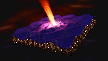
Image Caption: This cutaway view shows stripes of higher and lower electron density—“charge stripes”—within a copper-based superconducting material. Experiments with SLAC’s X-ray laser directly observed how those stripes fluctuate when hit with a pulse of light, a step toward understanding how they interact with high-temperature superconductivity. (Greg Stewart/SLAC National Accelerator Laboratory)
One piece of the puzzle is the fact that charge density waves – static stripes of higher and lower electron density running through a material—have been found in one of the major families of high-temperature superconductors, the copper-based cuprates. But do these charge stripes enhance superconductivity, suppress it or play some other role?
In independent studies, two research teams report important advances in understanding how charge stripes might interact with superconductivity. Both studies were carried out with X-rays at the Department of Energy’s SLAC National Accelerator Laboratory.
Exquisite Detail
In a paper published today in Science Advances, researchers from the University of Illinois at Urbana-Champaign (UIUC) used SLAC’s Linac Coherent Light Source (LCLS) X-ray free-electron laser to observe fluctuations in charge density waves in a cuprate superconductor.
They disturbed the charge density waves with pulses from a conventional laser and then used RIXS, or resonant inelastic X-ray scattering, to watch the waves recover over a period of a few trillionths of a second. This recovery process behaved according to a universal dynamical scaling law: It was the same at all scales, much as a fractal pattern looks the same whether you zoom in or zoom out.
With LCLS, the scientists were able to measure, for the first time and in exquisite detail, exactly how far and how fast the charge density waves fluctuated. To their surprise, the team discovered that the fluctuations were not like the ringing of a bell or the bouncing of a trampoline; instead, they were more like the slow diffusion of a syrup—a quantum analog of liquid crystal behavior, which had never been seen before in a solid.
“Our experiments at LCLS establish a new way to study fluctuations in charge density waves, which could lead to a new understanding of how high-temperature superconductors operate,” says Matteo Mitrano, a postdoctoral researcher in professor Peter Abbamonte’s group at UIUC.
This team also included researchers from Stanford University, the National Institute of Standards and Technology and Brookhaven National Laboratory.
Hidden Arrangements
Another study, reported last month in Nature Communications, used X-rays from SLAC’S Stanford Synchrotron Radiation Lightsource (SSRL) to discover two types of charge density wave arrangements, making a new link between these waves and high-temperature superconductivity.
Led by SLAC scientist Jun-Sik Lee, the research team used RSXS, or resonant soft X-ray scattering, to watch how temperature affected the charge density waves in a cuprate superconductor.
“This resolves a mismatch in data from previous experiments and charts a new course for fully mapping the behaviors of electrons in these exotic superconducting materials,” Lee says.
“I believe that exploring new or hidden arrangements, as well as their intertwining phenomena, will contribute to our understanding of high-temperature superconductivity in cuprates, which will inform researchers in their quest to design and develop new superconductors that work at warmer temperatures.”
The team also included researchers from Stanford, Pohang Accelerator Laboratory in South Korea and Tohoku University in Japan.
SSRL and LCLS are DOE Office of Science user facilities. Both studies were supported by the Office of Science.
Share on:


Suggested Items
Insulectro’s 'Storekeepers' Extend Their Welcome to Technology Village at IPC APEX EXPO
04/03/2024 | InsulectroInsulectro, the largest distributor of materials for use in the manufacture of PCBs and printed electronics, welcomes attendees to its TECHNOLOGY VILLAGE during this year’s IPC APEX EXPO at the Anaheim Convention Center, April 9-11, 2024.
ENNOVI Introduces a New Flexible Circuit Production Process for Low Voltage Connectivity in EV Battery Cell Contacting Systems
04/03/2024 | PRNewswireENNOVI, a mobility electrification solutions partner, introduces a more advanced and sustainable way of producing flexible circuits for low voltage signals in electric vehicle (EV) battery cell contacting systems.
Heavy Copper PCBs: Bridging the Gap Between Design and Fabrication, Part 1
04/01/2024 | Yash Sutariya, Saturn Electronics ServicesThey call me Sparky. This is due to my talent for getting shocked by a variety of voltages and because I cannot seem to keep my hands out of power control cabinets. While I do not have the time to throw the knife switch to the off position, that doesn’t stop me from sticking screwdrivers into the fuse boxes. In all honesty, I’m lucky to be alive. Fortunately, I also have a talent for building high-voltage heavy copper circuit boards. Since this is where I spend most of my time, I can guide you through some potential design for manufacturability (DFM) hazards you may encounter with heavy copper design.
Trouble in Your Tank: Supporting IC Substrates and Advanced Packaging, Part 5
03/19/2024 | Michael Carano -- Column: Trouble in Your TankDirect metallization systems based on conductive graphite or carbon dispersion are quickly gaining acceptance worldwide. Indeed, the environmental and productivity gains one can achieve with these processes are outstanding. In today’s highly competitive and litigious environment, direct metallization reduces costs associated with compliance, waste treatment, and legal issues related to chemical exposure. What makes these processes leaders in the direct metallization space?
AT&S Shines with Purest Copper on World Recycling Day
03/18/2024 | AT&SThe Styrian microelectronics specialist AT&S is taking World Recycling Day as an opportunity to review the progress that has been made in recent months at its sites around the world in terms of the efficient use of resources: