


 Marcy's Musings: The Growing Industry
 It’s Only Common Sense: Here’s What To Do After IPC APEX EXPO 2024
 Dan’s Biz Bookshelf: Seeing the How
Enhancing Materials for Hi-Res Patterning to Advance Microelectronics
August 29, 2019 | Brookhaven National LaboratoryEstimated reading time: 6 minutes
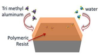
To increase the processing speed and reduce the power consumption of electronic devices, the microelectronics industry continues to push for smaller and smaller feature sizes. Transistors in today’s cell phones are typically 10 nanometers (nm) across—equivalent to about 50 silicon atoms wide—or smaller. Scaling transistors down below these dimensions with higher accuracy requires advanced materials for lithography—the primary technique for printing electrical circuit elements on silicon wafers to manufacture electronic chips. One challenge is developing robust “resists,” or materials that are used as templates for transferring circuit patterns into device-useful substrates such as silicon.
Now, scientists from the Center for Functional Nanomaterials (CFN)—a U.S. Department of Energy (DOE) Office of Science User Facility at Brookhaven National Laboratory—have used the recently developed technique of infiltration synthesis to create resists that combine the organic polymer poly(methyl methacrylate), or PMMA, with inorganic aluminum oxide. Owing to its low cost and high resolution, PMMA is the most widely used resist in electron-beam lithography (EBL), a kind of lithography in which electrons are used to create the pattern template. However, at the resist thicknesses that are necessary to generate the ultrasmall feature sizes, the patterns typically start to degrade when they are etched into silicon, failing to produce the required high aspect ratio (height to width).
As reported in a paper published online on July 8 in the Journal of Materials Chemistry C, these “hybrid” organic-inorganic resists exhibit a high lithographic contrast and enable the patterning of high-resolution silicon nanostructures with a high aspect ratio. By changing the amount of aluminum oxide (or a different inorganic element) infiltrated into PMMA, the scientists can tune these parameters for particular applications. For example, next-generation memory devices such as flash drives will be based on a three-dimensional stacking structure to increase memory density, so an extremely high aspect ratio is desirable; on the other hand, a very high resolution is the most important characteristic for future processor chips.
(Left to right): Ashwanth Subramanian, Ming Lu, Kim Kisslinger, Chang-Yong Nam, and Nikhil Tiwale in the Electron Microscopy Facility at Brookhaven Lab's Center for Functional Nanomaterials. The scientists used scanning electron microscopes to image high-resolution, high-aspect-ratio silicon nanostructures they etched using a "hybrid" organic-inorganic resist.
“Instead of taking an entirely new synthesis route, we used an existing resist, an inexpensive metal oxide, and common equipment found in almost every nanofabrication facility,” said first author Nikhil Tiwale, a postdoctoral research associate in the CFN Electronic Nanomaterials Group.
Though other hybrid resists have been proposed, most of them require high electron doses (intensities), involve complex chemical synthesis methods, or have expensive proprietary compositions. Thus, these resists are not optimal for the high-rate, high-volume manufacture of next-generation electronics.
Page 1 of 3
Share on:


Suggested Items
D Coupon Testing and Data Insights With GreenSource Fabrication
04/17/2024 | Marcy LaRont, PCB007 MagazineMarcy LaRont spoke with Steve Karas of GreenSource Fabrication at the SMTA UHDI conference in March. He presented a case study that GreenSource undertook with a customer on critical via reliability with advanced materials and used the experience to highlight the importance and effectiveness of D coupon testing. He also discussed GreenSource’s approach to data aggregation and a new system they developed to use collected data effectively.
IPC Publishes Comprehensive Strategy to Address Electronics Industry’s Global Workforce Challenge
04/10/2024 | IPCOne of the most difficult and urgent challenges facing the electronics industry is a chronic shortage of adequately skilled workers. Today, IPC unveiled an expansion of its strategy to address the workforce challenges of the U.S. electronics manufacturing industry and called on its more than 3,000 member companies to join in the effort.
UHDI Fundamentals: ASC Sponsors Ultra High Density Interconnect Symposium
03/21/2024 | Anaya Vardya, American Standard CircuitsAmerican Standard Circuits (ASC) is a major sponsor of an upcoming symposium on one of the most talked about new technologies that has come along in quite a while: ultra high density interconnect (UHDI).
onsemi Aligns Business Groups to Expand Product Portfolio and Accelerate Growth
03/13/2024 | onsemionsemi announced the formation of the Analog and Mixed-Signal Group (AMG) which will be led by newly appointed group president, Sudhir Gopalswamy.
Indium Corporation Experts to Present at SEMI THERM
03/07/2024 | Indium CorporationIndium Corporation Global Account Manager and Senior Thermal Technologist Tim Jensen and Product Development Specialist for Thermal Interface Materials Miloš Lazić will present on thermal interface material (TIM) technology at SEMI-THERM, taking place March 25–28 in San Jose, California, U.S.