


 Marcy's Musings: The Growing Industry
 It’s Only Common Sense: Here’s What To Do After IPC APEX EXPO 2024
 Dan’s Biz Bookshelf: Seeing the How
Borophene on Silver Grows Freely into an Atomic ‘Skin’
September 30, 2019 | Rice UniversityEstimated reading time: 4 minutes
Borophene has a nearly perfect partner in a form of silver that could help the trendy two-dimensional material grow to unheard-of lengths.
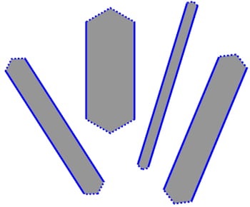
Image Caption: Models by materials scientists at Rice University and their colleagues suggest a method to control the growth of valuable two-dimensional borophene. The model predicts a variety of possible shapes of the 2D boron flakes with different aspect ratios, including thin ribbons. (Credit: Zhuhua Zhang/Rice University/Nanjing University of Aeronautics and Astronautics)
A well-ordered lattice of silver atoms makes it possible to speed the growth of pristine borophene, the atom-thick allotrope of boron that so far can only form via synthesis by molecular-beam epitaxy (MBE).
By using a silver substrate and through careful manipulation of temperature and deposition rate, scientists have discovered they can grow elongated hexagon-shaped flakes of borophene. They suggested the use of a proper metal substrate could facilitate the growth of ultrathin, narrow borophene ribbons.
New work published in Science Advances by researchers at Rice and Northwestern universities, Nanjing University of Aeronautics and Astronautics and Argonne National Laboratory will help streamline the manufacture of the conductive material, which shows potential for use in wearable and transparent electronics, plasmonic sensors and energy storage.
An illustration shows how edges are connected at the corners of a borophene flake. Materials scientists led by Rice University have predicted that the shape of borophene, the 2D allotrope of boron, can be controlled. (Credit: Zhuhua Zhang/Rice University/Nanjing University of Aeronautics and Astronautics)
That potential has fueled efforts to make it easier to grow, led by Rice materials scientist Boris Yakobson, a theorist who predicted that borophene could be synthesized. He and collaborators Mark Hersam at Northwestern and lead author Zhuhua Zhang, a Rice alumnus and now a professor at Nanjing, have now demonstrated through theory and experimentation that large-scale, high-quality samples of borophene are not only possible but also allow qualitative understanding of their growth patterns.
Unlike the repeating atomic lattices found in graphene and hexagonal boron nitride, borophene incorporates a regular, woven-in array of “vacancies,” missing atoms that leave hexagonal holes among the triangles. This not only affects the material’s electronic properties but also influences how new atoms join the flake as it is being formed.
The Yakobson lab’s calculations showed the edge energies — atoms that are less stable along the edges of 2D materials than those in the interior — are significantly lower than those in graphene and boron nitride and that the conditions can be manipulated to tune the edges for optimum growth of ribbons.
Initial calculations showed borophene in equilibrium should form as a rectangle, but experiments proved otherwise.
The confounding factor was in the flake’s edges that, forced by the vacancies, appear in variations of zigzag and armchair configurations. Atoms settle one by one into the “kinks” that appear along the edges, but as armchairs are more energetically stable and present a higher barrier to the atoms, they prefer to join the zigzags. Rather than extending the flakes in all directions, the atoms are selective about where they settle and elongate the structure instead.
“On the atomic scale, edges don’t act as though you cut the lattice with a pair of scissors,” Yakobson said. “The dangling bonds you create reconnect with their neighbors, and the edge atoms adapt slightly different, reconstructed configurations.
“So the origin of the shapes must not lie in equilibrium,” he said. “They are caused by the kinetics of growth, how fast or slow the side edges advance. Opportunely, we had developed a theoretical framework for graphene, a nanoreactor model that works for other 2D materials, including boron.”
Controlling the flow of atoms as well as temperature gives the researchers a simpler way to control borophene synthesis.
“Silver (111) provides a landing for boron atoms, which then diffuse along the surface to find the edges of a growing borophene flake,” Zhang said. “Upon arrival, the boron atoms are lifted onto the edges by silver, but how difficult such a lift is depends on the edge’s orientation. As a result, a pair of opposite zigzag edges grow very slowly while all other edges grow very fast, manifested as an elongation of the boron flake.”
The researchers said the ability to grow needlelike ribbons of borophene gives them the potential to serve as atom-width conductive wires for nanoelectronics devices.
“Graphene-based electronics that have been conceived so far mostly rely on ribbonlike building blocks,” Yakobson said. “Metallic boron ribbons with high conductivity will be a natural match as interconnects in circuitry.”
Co-authors of the paper are Xiaolong Liu of Northwestern, Nathan Guisinger of Argonne’s Center for Nanoscale Materials, Andrew Mannix of Argonne and Northwestern, and Zhili Hu of Nanjing and Rice. Yakobson is the Karl F. Hasselmann Professor of Materials Science and NanoEngineering and a professor of chemistry at Rice. Hersam is the Walter P. Murphy Professor of Materials Science and Engineering at Northwestern.
The National Natural Science Foundation of China, the State Key Laboratory of Mechanics and Control of Mechanical Structures, the Department of Energy, the Office of Naval Research and the National Science Foundation supported the research.
Share on:


Suggested Items
Groundbreaking Ceremony Marks the Beginning of a New Era for Newccess Industrial; The Construction of the MINGXIN Building
04/12/2024 | Newccess IndustrialOn a clear and sunny day in March, the groundbreaking ceremony for the MINGXIN Building took place in Shenzhen, China. This moment marked the official commencement of construction for a project that will reshape the semiconductor materials industry.
The Need for a Holistic Global Sustainability Standard
04/10/2024 | Michael Ford, Aegis SoftwareNo one can deny that the resources of our fragile planet are finite. The environment seems like a third party, subject to constant degradation. We’re acutely aware of the effects of pollution on our climate, and despite our “throw-away” culture, recycling and recovery of materials has remained relatively expensive, even as we use more energy just to survive.
iNEMI Publishes Four Roadmap Topics
04/04/2024 | iNEMIThe International Electronics Manufacturing Initiative (iNEMI) announces the availability of the first roadmap topics in the new iNEMI Roadmap format. Printed circuit boards, sustainable electronics, smart manufacturing, and mmWave materials and test are now available online.
Insulectro’s 'Storekeepers' Extend Their Welcome to Technology Village at IPC APEX EXPO
04/03/2024 | InsulectroInsulectro, the largest distributor of materials for use in the manufacture of PCBs and printed electronics, welcomes attendees to its TECHNOLOGY VILLAGE during this year’s IPC APEX EXPO at the Anaheim Convention Center, April 9-11, 2024.
Checking In With ICAPE Group
04/03/2024 | Nolan Johnson, I-Connect007ICAPE Group’s field application engineer Erik Pederson drills down on sustainability, supply chain resiliency, and what value engineering really looks like in this exclusive interview. Founded in 1999, European-based ICAPE Group provides 21 million printed circuit boards and over six million technical parts to manufacturers every month. With 30 PCB manufacturing partners globally and 50 partners providing a wide array of technical parts, ICAPE Group has operations in China, Taiwan, Thailand, South Korea, Vietnam, South Africa, Europe, Mexico, and the United States. The company also focuses on the value proposition for its customers.