


 It’s Only Common Sense: OCCAM—the Time Is Now
 Marcy's Musings: The Growing Industry
 Dan’s Biz Bookshelf: Seeing the How
Silicon Technology Boost with Graphene and 2D Materials
October 1, 2019 | ICFOEstimated reading time: 2 minutes
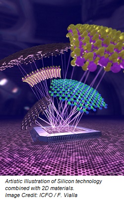
Silicon semiconductor technology has done marvels for the advancement of our society, who has benefited tremendously from its versatile use and amazing capabilities. The development of electronics, automation, computers, digital cameras and recent smartphones based on this material and its underpinning technology has reached skyrocket limits, downscaling the physical size of devices and wires to the nanometre regime.
Although this technology has been developing since the late 1960s, the miniaturization of circuits seems to have reached a possible halt, since transistors can only be shrunk down to a certain size and not further beyond. Thus, there is a pressing need to complement Si CMOS technology with new materials, and fulfil the future computing requirements as well as the needs for diversification of applications.
Now, graphene and related two-dimensional (2D) materials offer prospects of unprecedented advances in device performance at the atomic limit. Their amazing potential has proven to be a possible solution to overcome the limitations of silicon technology, where the combination of 2D materials with silicon chips promises to surpass the current technological limitations.
In the new review article in Nature, a team of international researchers including ICFO researchers Dr. Stijn Goossens and ICREA Prof at ICFO Frank Koppens, and industrial leaders from IMEC and TSMC have come together to provide an in-depth and thorough review about the opportunities, progress and challenges of integrating atomically thin materials with Si-based technology. They give insights on how and why 2D materials (2DMs) could overcome current challenges posed by the existing technology and how they can enhance both device component function and performance, to boost the features of future technologies, in the areas of computational and non-computational applications.
For non-computational applications, they review the possible integration of these materials for future cameras, low power optical data communications and gas and bio-sensors. In particular, image sensors and photodetectors, where graphene and 2DMs could enable a new vision in the infrared and terahertz range in addition to the visible range of the spectrum. These can serve for example in autonomous vehicle, security at airports and augmented reality.
For computational systems, and in particular in the field of transistors, they show how challenges such as doping, contact resistance and dielectrics/encapsulation can be diminished when integrating 2DMs with Si technology. 2DMs could also radically improve memory and data storage devices with novel switching mechanisms for meta-insulator-metal structures, avoid sneak currents in memory arrays, or even push performance gains of copper wired based circuitry by adhering graphene to the ultrathin copper barrier materials and thus reduce resistance, scattering and self-heating.
The review provides insight to all stakeholders about the challenges and impact of solving the 2D material integration with CMOS technology. It provides a roadmap of 2D integration and CMOS technology, pinpointing the stage at which all challenges regarding growth, transfer, interface, doping, contacting, and design are currently standing today and what possible processes are expected to be resolved to achieve such goals of moving from a research laboratory environment to a pilot line for production of the first devices that combine both technologies.
The first 2D material-CMOS roadmap, as presented in this review, gives an exciting glimpse in the future, with first pilot production to be expected already in just a few years from now.
Share on:


Suggested Items
Insulectro’s 'Storekeepers' Extend Their Welcome to Technology Village at IPC APEX EXPO
04/03/2024 | InsulectroInsulectro, the largest distributor of materials for use in the manufacture of PCBs and printed electronics, welcomes attendees to its TECHNOLOGY VILLAGE during this year’s IPC APEX EXPO at the Anaheim Convention Center, April 9-11, 2024.
ENNOVI Introduces a New Flexible Circuit Production Process for Low Voltage Connectivity in EV Battery Cell Contacting Systems
04/03/2024 | PRNewswireENNOVI, a mobility electrification solutions partner, introduces a more advanced and sustainable way of producing flexible circuits for low voltage signals in electric vehicle (EV) battery cell contacting systems.
Heavy Copper PCBs: Bridging the Gap Between Design and Fabrication, Part 1
04/01/2024 | Yash Sutariya, Saturn Electronics ServicesThey call me Sparky. This is due to my talent for getting shocked by a variety of voltages and because I cannot seem to keep my hands out of power control cabinets. While I do not have the time to throw the knife switch to the off position, that doesn’t stop me from sticking screwdrivers into the fuse boxes. In all honesty, I’m lucky to be alive. Fortunately, I also have a talent for building high-voltage heavy copper circuit boards. Since this is where I spend most of my time, I can guide you through some potential design for manufacturability (DFM) hazards you may encounter with heavy copper design.
Trouble in Your Tank: Supporting IC Substrates and Advanced Packaging, Part 5
03/19/2024 | Michael Carano -- Column: Trouble in Your TankDirect metallization systems based on conductive graphite or carbon dispersion are quickly gaining acceptance worldwide. Indeed, the environmental and productivity gains one can achieve with these processes are outstanding. In today’s highly competitive and litigious environment, direct metallization reduces costs associated with compliance, waste treatment, and legal issues related to chemical exposure. What makes these processes leaders in the direct metallization space?
AT&S Shines with Purest Copper on World Recycling Day
03/18/2024 | AT&SThe Styrian microelectronics specialist AT&S is taking World Recycling Day as an opportunity to review the progress that has been made in recent months at its sites around the world in terms of the efficient use of resources: