


 The Right Approach: I Hear the Train A Comin'
 It’s Only Common Sense: OCCAM—the Time Is Now
 Marcy's Musings: The Growing Industry
Gift Will Allow MIT Researchers to Use Artificial Intelligence in a Biomedical Device
January 29, 2020 | MITEstimated reading time: 1 minute
Researchers in the MIT Department of Civil and Environmental Engineering (CEE) have received a gift to advance their work on a device designed to position living cells for growing human organs using acoustic waves. The Acoustofluidic Device Design with Deep Learning is being supported by Natick, Massachusetts-based MathWorks, a leading developer of mathematical computing software.
“One of the fundamental problems in growing cells is how to move and position them without damage,” says John R. Williams, a professor in CEE. “The devices we’ve designed are like acoustic tweezers.”
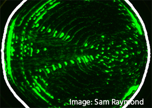
Inspired by the complex and beautiful patterns in the sand made by waves, the researchers' approach is to use sound waves controlled by machine learning to design complex cell patterns. The pressure waves generated by acoustics in a fluid gently move and position the cells without damaging them.
The engineers developed a computer simulator to create a variety of device designs, which were then fed to an AI platform to understand the relationship between device design and cell positions.
“Our hope is that, in time, this AI platform will create devices that we couldn’t have imagined with traditional approaches,” says Sam Raymond, who recently completed his doctorate working with Williams on this project. Raymond’s thesis title, "Combining Numerical Simulation and Machine Learning," explored the application of machine learning in computational engineering.
“MathWorks and MIT have a 30-year long relationship that centers on advancing innovations in engineering and science,” says P.J. Boardman, director of MathWorks. “We are pleased to support Dr. Williams and his team as they use new methodologies in simulation and deep learning to realize significant scientific breakthroughs.”
Williams and Raymond collaborated with researchers at the University of Melbourne and the Singapore University of Technology and Design on this project.
Share on:


Suggested Items
iNEMI Packaging Tech Topic Series: Role of EDA in Advanced Semiconductor Packaging
04/26/2024 | iNEMIAdvanced semiconductor packaging with heterogenous integration has made on-package integration of multiple chips a crucial part of finding alternatives to transistor scaling. Historically, EDA tools for front-end and back-end design have evolved separately; however, design complexity and the increased number of die-to-die or die-to-substrate interconnections has led to the need for EDA tools that can support integration of overall design planning, implementation, and system analysis in a single cockpit.
Cadence, TSMC Collaborate on Wide-Ranging Innovations to Transform System and Semiconductor Design
04/25/2024 | Cadence Design SystemsCadence Design Systems, Inc. and TSMC have extended their longstanding collaboration by announcing a broad range of innovative technology advancements to accelerate design, including developments ranging from 3D-IC and advanced process nodes to design IP and photonics.
Ansys, TSMC Enable a Multiphysics Platform for Optics and Photonics, Addressing Needs of AI, HPC Silicon Systems
04/25/2024 | PRNewswireAnsys announced a collaboration with TSMC on multiphysics software for TSMC's Compact Universal Photonic Engines (COUPE). COUPE is a cutting-edge Silicon Photonics (SiPh) integration system and Co-Packaged Optics platform that mitigates coupling loss while significantly accelerating chip-to-chip and machine-to-machine communication.
Siemens’ Breakthrough Veloce CS Transforms Emulation and Prototyping with Three Novel Products
04/24/2024 | Siemens Digital Industries SoftwareSiemens Digital Industries Software launched the Veloce™ CS hardware-assisted verification and validation system. In a first for the EDA (Electronic Design Automation) industry, Veloce CS incorporates hardware emulation, enterprise prototyping and software prototyping and is built on two highly advanced integrated circuits (ICs) – Siemens’ new, purpose-built Crystal accelerator chip for emulation and the AMD Versal™ Premium VP1902 FPGA adaptive SoC (System-on-a-chip) for enterprise and software prototyping.
Listen Up! The Intricacies of PCB Drilling Detailed in New Podcast Episode
04/25/2024 | I-Connect007In episode 5 of the podcast series, On the Line With: Designing for Reality, Nolan Johnson and Matt Stevenson continue down the manufacturing process, this time focusing on the post-lamination drilling process for PCBs. Matt and Nolan delve into the intricacies of the PCB drilling process, highlighting the importance of hole quality, drill parameters, and design optimization to ensure smooth manufacturing. The conversation covers topics such as drill bit sizes, aspect ratios, vias, challenges in drilling, and ways to enhance efficiency in the drilling department.