


 The Right Approach: I Hear the Train A Comin'
 It’s Only Common Sense: OCCAM—the Time Is Now
 Marcy's Musings: The Growing Industry
Compound Photonics Backplane Enables World’s Smallest MicroLED AR Displays
May 5, 2020 | Business WireEstimated reading time: 2 minutes
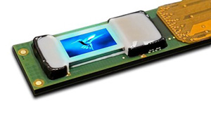
Compound Photonics US Corporation (CP), a global leader providing compact high-resolution microdisplay solutions for Augmented and Mixed Reality (AR/MR), announces today the wide availability of its high-performance digital backplane to leading microLED developers worldwide for integration into complete microdisplay subsystems.
CP re-engineered its market-ready LCoS backplane technology into an innovative constant current drive configuration for microLED pixels based on its industry-leading 0.26” diagonal (~3 ?m pixel) 1080p display format. microLED developers can accelerate their time to market by bonding their devices to a backplane driven by CP’s field-proven NOVA display drive architecture to enable complete display subsystems meeting critical AR requirements for compactness, optical performance and brightness with high frame rate, low latency and low power consumption.
“Our custom, constant current pixel circuit design provides greater tolerance to forward voltage variation and IR drops in the microLED array resulting in a previously unattainable level of uniformity. It additionally features globally on-the-fly programmable pixel current control that greatly increases the system bandwidth, enabling higher frame rates while maintaining full bit depth,” commented Ian Kyles, CP Vice President of Electrical/Software Engineering. “The backplane also has additional steering pixels beyond its native 2048x1080 resolution to enhance alignment/integration of the display within the optical system.”
MicroLED developers using this backplane can access CP’s monolithic integrated display module (IDM) (7.25 x 15.5 x 3.1 mm) with a low pin count interconnect and a direct MIPI input packaged into a compact subsystem amenable to smaller optical engine size. The IDM integrates CP’s proprietary NOVA drive architecture’s software defined platform to enable customizable frame-by-frame control of video frame rates (up to 240 Hz), bit depth, and other parameters to optimize for low latency, short persistence and low power while maintaining near 100% duty cycle according to type of image content and use case.
Andrew Shih, CP’s Marketing and Business Development Manager continued, “Process integration compatibility is also important, as bonding of the microLED array to the backplane requires a highly planar interface. CP’s backplane wafers feature excellent planarity, a direct benefit from extensive process tuning work to meet earlier LCoS requirements. By partnering with CP, whose backplane technology facilitates both wafer level process integration and a direct path to a complete NOVA-based microdisplay subsystem solution, microLED developers can focus on their core competencies in compound semiconductor photonic device engineering and process development while reducing development time and cost.”
A provisional backplane reference specification is presently available for customer review and CP is currently accepting engagements with leading microLED developers.
Share on:


Suggested Items
Koh Young Showcases Award-winning Inspection Solutions at SMTconnect with SmartRep in Hall 4A.225
04/25/2024 | Koh Young TechnologyKoh Young Technology, the industry leader in True 3D measurement-based inspection solutions, will showcase an array of award-winning inspection and measurement solutions at SMTconnect alongside its sales partner, SmartRep, in booth 4A.225 at NürnbergMesse from June 11-13, 2023. The following offers a glimpse into what Koh Young will present at the tradeshow:
Real Time with… IPC APEX EXPO 2024: Plasmatreat: Innovative Surface Preparation Solutions
04/25/2024 | Real Time with...IPC APEX EXPOIn this interview, Editor Nolan Johnson speaks with Hardev Grewal, CEO and president of Plasmatreat, a developer of atmospheric plasma solutions. Plasmatreat uses clean compressed air and electricity to create plasma, offering environmentally friendly methods for surface preparation. Their technology measures plasma density for process optimization and can remove organic micro-contamination. Nolan and Hardev also discuss REDOX-Tool, a new technology for removing metal oxides.
KYZEN to Promote Pair of Stencil Cleaning Chemistries at SMTA Ciudad Jaurez Expo & Tech Forum
04/25/2024 | KYZEN'KYZEN, the global leader in innovative environmentally friendly cleaning chemistries, will exhibit at the SMTA Ciudad Juarez Expo & Tech Forum, scheduled to take place Thursday, May 9, 2024 at the Injectronic Convention Center in Ciudad Jaurez, Chihuahua, Mexico. During the event the KYZEN Clean Team will focus on understencil cleaning products KYZEN E5631J and CYBERSOLV C8882.
Cadence, TSMC Collaborate on Wide-Ranging Innovations to Transform System and Semiconductor Design
04/25/2024 | Cadence Design SystemsCadence Design Systems, Inc. and TSMC have extended their longstanding collaboration by announcing a broad range of innovative technology advancements to accelerate design, including developments ranging from 3D-IC and advanced process nodes to design IP and photonics.
Listen Up! The Intricacies of PCB Drilling Detailed in New Podcast Episode
04/25/2024 | I-Connect007In episode 5 of the podcast series, On the Line With: Designing for Reality, Nolan Johnson and Matt Stevenson continue down the manufacturing process, this time focusing on the post-lamination drilling process for PCBs. Matt and Nolan delve into the intricacies of the PCB drilling process, highlighting the importance of hole quality, drill parameters, and design optimization to ensure smooth manufacturing. The conversation covers topics such as drill bit sizes, aspect ratios, vias, challenges in drilling, and ways to enhance efficiency in the drilling department.