


 The Right Approach: I Hear the Train A Comin'
 It’s Only Common Sense: OCCAM—the Time Is Now
 Marcy's Musings: The Growing Industry
Siemens Automates 2.5D, 3D IC Design-for-test with New Tessent Multi Die Solution
September 26, 2022 | SiemensEstimated reading time: 2 minutes
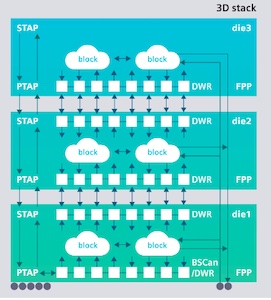
Siemens Digital Industries Software introduced the Tessent Multi-die software solution, which helps customers dramatically speed and simplify critical design-for-test (DFT) tasks for next-generation integrated circuits (ICs) based on 2.5D and 3D architectures.
As demand for smaller, more power efficient and higher performing ICs continues to challenge the global IC design community, next-generation devices increasingly feature complex 2.5D and 3D architectures that connect dies vertically (3D IC) or side-by-side (2.5D) so that they behave as a single device. However, these approaches can present significant challenges for IC test, since most legacy IC test approaches are based on conventional two-dimensional processes.
To address these challenges, Siemens today introduces Tessent Multi-die software -- the industry’s most comprehensive DFT automation solution for highly complex DFT tasks associated with 2.5D and 3D IC designs. The new solution works seamlessly with Siemens’ Tessent™ TestKompress™ Streaming Scan Network software and Tessent™ IJTAG software, which optimize DFT test resources for each block without concern for impacts to the rest of the design, thereby streamlining DFT planning and implementation for the 2.5D and 3D IC era. Using Tessent Multi-die software, IC design teams can rapidly generate IEEE 1838 compliant hardware featuring 2.5D and 3D IC architectures.
“IC design organizations are seeing dramatic spikes in IC test complexity due to the rapid adoption and deployment of designs featuring densely packed dies in 2.5D and 3D devices,” said Ankur Gupta, vice president and general manager of the Tessent business unit for Siemens Digital Industries Software. “With Siemens’ new Tessent Multi-die solution, our customers can be ready for the designs of tomorrow, while slashing test implementation effort and simultaneously optimizing manufacturing test cost today.”
In addition to supporting comprehensive test for 2.5D and 3D IC designs, the Tessent Multi-die solution can generate die-to-die interconnect patterns and enable package level test using the Boundary Scan Description Language (BSDL). Further, Tessent Multi-die supports integration of flexible parallel port (FPP) technology by leveraging the packetized data delivery capabilities of Siemens’ Tessent TestKompress Streaming Scan Network software. Introduced two years ago, Tessent TestKompress Streaming Scan Network decouples core-level DFT requirements from the chip-level test delivery resources. This enables a no-compromise, bottom-up DFT flow that can dramatically simplify DFT planning and implementation, while reducing test time up to 4X.
“As the limits of traditional 2D IC design approaches become increasingly clear over time, more design teams are leveraging the power, performance and form factor advantages that 2.5D and 3D IC architectures can deliver. But deploying these advanced schemes in new design starts without first establishing a DFT strategy that acknowledges the inherent challenges these architectures present can raise costs and undermine aggressive timelines,” said Laurie Balch, president and research director for Pedestal Research. “However, by evolving DFT technology to keep pace with the rapid adoption of multi-dimensional designs, EDA vendors can play a key role in further enabling global, mainstream adoption of 2.5D and 3D architectures.”
Share on:


Suggested Items
iNEMI Packaging Tech Topic Series: Role of EDA in Advanced Semiconductor Packaging
04/26/2024 | iNEMIAdvanced semiconductor packaging with heterogenous integration has made on-package integration of multiple chips a crucial part of finding alternatives to transistor scaling. Historically, EDA tools for front-end and back-end design have evolved separately; however, design complexity and the increased number of die-to-die or die-to-substrate interconnections has led to the need for EDA tools that can support integration of overall design planning, implementation, and system analysis in a single cockpit.
Cadence, TSMC Collaborate on Wide-Ranging Innovations to Transform System and Semiconductor Design
04/25/2024 | Cadence Design SystemsCadence Design Systems, Inc. and TSMC have extended their longstanding collaboration by announcing a broad range of innovative technology advancements to accelerate design, including developments ranging from 3D-IC and advanced process nodes to design IP and photonics.
Ansys, TSMC Enable a Multiphysics Platform for Optics and Photonics, Addressing Needs of AI, HPC Silicon Systems
04/25/2024 | PRNewswireAnsys announced a collaboration with TSMC on multiphysics software for TSMC's Compact Universal Photonic Engines (COUPE). COUPE is a cutting-edge Silicon Photonics (SiPh) integration system and Co-Packaged Optics platform that mitigates coupling loss while significantly accelerating chip-to-chip and machine-to-machine communication.
Siemens’ Breakthrough Veloce CS Transforms Emulation and Prototyping with Three Novel Products
04/24/2024 | Siemens Digital Industries SoftwareSiemens Digital Industries Software launched the Veloce™ CS hardware-assisted verification and validation system. In a first for the EDA (Electronic Design Automation) industry, Veloce CS incorporates hardware emulation, enterprise prototyping and software prototyping and is built on two highly advanced integrated circuits (ICs) – Siemens’ new, purpose-built Crystal accelerator chip for emulation and the AMD Versal™ Premium VP1902 FPGA adaptive SoC (System-on-a-chip) for enterprise and software prototyping.
Listen Up! The Intricacies of PCB Drilling Detailed in New Podcast Episode
04/25/2024 | I-Connect007In episode 5 of the podcast series, On the Line With: Designing for Reality, Nolan Johnson and Matt Stevenson continue down the manufacturing process, this time focusing on the post-lamination drilling process for PCBs. Matt and Nolan delve into the intricacies of the PCB drilling process, highlighting the importance of hole quality, drill parameters, and design optimization to ensure smooth manufacturing. The conversation covers topics such as drill bit sizes, aspect ratios, vias, challenges in drilling, and ways to enhance efficiency in the drilling department.