


 Marcy's Musings: The Growing Industry
 It’s Only Common Sense: Here’s What To Do After IPC APEX EXPO 2024
 Dan’s Biz Bookshelf: Seeing the How
Advanced Semiconductor Packaging Technologies: The Development Trend and the Growth Drivers, IDTechEx Reports
May 15, 2023 | PRNewswireEstimated reading time: 3 minutes
Advanced semiconductor packaging technologies are crucial due to the slowing of Moore's law and rising costs of monolithic Si IC development and manufacturing. Initially, components were individually packaged and integrated at the PCB board level, but as devices become smaller and require higher processing capabilities, component integration needs to be pushed beyond board level. Package level integration was the first advancement, followed by wafer level integration, which provides at least ten times higher connection density, a smaller footprint suitable for size-sensitive applications, and superior performance.
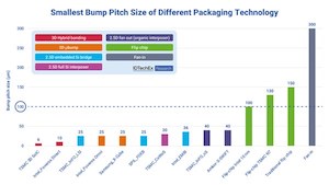
Wafer level integration encompasses fan-in, core fan-out, high-density fan-out, 2.5D IC, and 3D IC packaging technologies. However, only those with a bumping pitch size of less than 100 µm are considered as "advanced" semiconductor packaging technologies. This includes high-density fan-out, 2.5D IC, and 3D IC packaging technologies.
The shift from 2.5D hybrid integration to complete 3D vertical integration is crucial for future data-centric applications, and in this article, we will focus on this transition.
The primary challenge in the shift from 2.5D to 3D is to scale the size of the bumping pitch. In a 2.5D IC package, the bump pitch size ranges between 25 µm and 40 µm, depending on the interposer material. However, for a 3D stacking package, the bump size must be scaled down to a single digit µm or even lower down to below 1 µm dimension. TSMC has reported that the bump pitch for stacking N7/N6 chips is 9 µm and 6 µm for N5 chips stacking. This is expected to further decrease to 4.5 µm for N3 chip stacking and continue to decline for future generations of ICs. Stacking two chips with a small bump pitch size poses a significant challenge, as high-precision alignment on bonding dielectric materials must be achieved, especially at low temperatures. Additionally, proper control of Cu filling materials is necessary to prevent overflow during the bonding process. Furthermore, thermal management becomes a critical issue for packages with small bumping scales, which necessitates the consideration of package designs that enable better heat transmission and possible liquid cooling technologies.
The Growth Drivers
IDTechEx has identified four main application areas for advanced semiconductor packaging: high-performance computing (HPC) applications/data centers, communication networks, autonomous cars, and consumer electronics. The increasing demand for data processing is the primary driving force behind the growth in these application areas. However, each application has specific requirements that necessitate different advanced semiconductor packaging technologies.
For HPC applications/data centers, the priority is to provide superior data processing capabilities, making 2.5DIC technologies that use Si interposer or Si bridge the preferred option, despite their higher cost. In contrast, consumer electronics such as smartphones or smartwatches focus on miniaturization and cost, with organic-based packaging technologies being the top choice.
In 5G and beyond communication, the key challenge is transmission loss. Hence, advanced packaging technologies are used to bring the antenna closer to the RF IC chip, minimizing transmission loss. "Antenna-in-package (AiP)" is currently the most viable option for 5G mmWave, while "Antenna on chip/wafer (AoP)" is still under intense development to reduce costs.
For future autonomous vehicles, heterogeneous integration of CPUs and other components, such as HBM and reliable power delivery systems, will create new opportunities for advanced semiconductor packaging and innovation.
The expansion of data processing is the unifying growth factor for all these applications. However, as the requirements for each application area differ, advanced semiconductor packaging technologies are being used to meet specific needs.
IDTechEx has released a new market research study titled "Advanced Semiconductor Packaging 2023-2033". This study examines the market prospects, key player analysis, and most recent developments in advanced semiconductor packaging technologies. This report also conducts a comprehensive examination of the semiconductor market as a whole. Additionally, IDTechEx leverages its expertise and years of research in data centers, autonomous vehicles, 5G, and consumer electronics to provide the reader with a thorough understanding of how advanced semiconductor packaging is influencing various industries and what the future may hold.
Share on:


Suggested Items
D Coupon Testing and Data Insights With GreenSource Fabrication
04/17/2024 | Marcy LaRont, PCB007 MagazineMarcy LaRont spoke with Steve Karas of GreenSource Fabrication at the SMTA UHDI conference in March. He presented a case study that GreenSource undertook with a customer on critical via reliability with advanced materials and used the experience to highlight the importance and effectiveness of D coupon testing. He also discussed GreenSource’s approach to data aggregation and a new system they developed to use collected data effectively.
Real Time with... IPC APEX EXPO 2024: Innovations in Thermal, Warpage, and Strain Metrology
04/17/2024 | Real Time with...IPC APEX EXPOEditor Nolan Johnson talks with Neil Hubble, president of Akrometrix, about the company's leadership in thermal, warpage, and strain metrology. Neil details how Akrometrix is committed to addressing customer challenges through technological evolution, innovative solutions, and a focus on data processing. A tabletop unit for thermal warpage testing is showcased at IPC APEX EXPO this year.
Signal Integrity Expert Donald Telian to Teach 'Signal Integrity, In Practice' Masterclass Globally
04/17/2024 | PRLOGDonald Telian and The EEcosystem announce the global tour of "Signal Integrity, In Practice," a groundbreaking LIVE masterclass designed to equip hardware engineers with essential skills for solving Signal Integrity (SI) challenges in today's fast-paced technological landscape.
SMT Prospects and Perspectives: AI Opportunities, Challenges, and Possibilities, Part 1
04/17/2024 | Dr. Jennie Hwang -- Column: SMT Perspectives and ProspectsIn this installment of my artificial intelligence (AI) series, I will touch on the key foundational technologies that propel and drive the development and deployment of AI, with special consideration of electronics packaging and assembly.
Argonne, RIKEN Sign a Memorandum of Understanding in Support of AI for Science
04/16/2024 | BUSINESS WIRELeaders in high performance computing in the U.S. and Japan have signed a memorandum of understanding (MOU) establishing a cooperative relationship in support of artificial intelligence (AI) computing projects.