


 It’s Only Common Sense: OCCAM—the Time Is Now
 Marcy's Musings: The Growing Industry
 Dan’s Biz Bookshelf: Seeing the How
3D Plasmon Antenna Capable of Focusing Light into Few Nanometers
June 26, 2015 | KAISTEstimated reading time: 1 minute
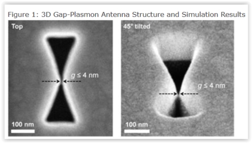
Professors Myung-Ki Kim and Yong-Hee Lee, both of the Physics Department at KAIST, and their research teams have developed a three dimensional (3D) gap-plasmon antenna which can focus light into a space a few nanometers wide. Their research findings were published in the June 10th issue of Nano Letters.
Focusing light into a point-like space is an active research field with many applications. However, concentrating light into a smaller space than its wavelength is often hindered by diffraction. To tackle this problem, many researchers have utilized the plasmonic phenomenon of a metal where light can be confined to a greater extent by overcoming the diffraction limit.
Many researchers have focused on developing a two dimensional (2D) plasmon antenna and were able to focus a light under 5 nanometers wide. However, this 2D antenna revealed a challenge: the light disperses to the opposite end regardless of how small its beam was focused. To solve this difficulty, a 3D structure had to be employed to maximize the light's intensity.
Adopting the proximal focused-ion-beam milling technology, the KAIST research team developed a 3D four nanometer wide gap-plasmon antenna. By squeezing the photons into a 3D nano space of 4 x 10 x 10 nm3 size, the researchers were able to increase the intensity of light by 400,000 times stronger than that of the incident light. Capitalizing on the enhanced intensity of light within the antenna, they intensified the second-harmonic signal and verified that the light was focused in the nano gap by scanning cathodoluminescent images.
The researchers anticipate that this technology will improve the speed of data transfer and processing up to the level of a terahertz (one trillion times per second) and to enlarge the storage volume per unit area on hard disks by 100 times. In addition, high definition images of submolecule size can be taken with actual light, instead of with an electron microscope, while improving the semiconductor process to a smaller size of few nanometers.
Professor Kim said, “A simple yet ingenious idea has shifted the research paradigm from 2D gap-plasmon antennas to 3D antennas. This technology will see numerous applications including in the field of information technology, data storage, imaging medical science, and semiconductor processes.”
The research was sponsored by the National Research Foundation of Korea.
Share on:


Suggested Items
SMC Korea 2024 to Highlight Semiconductor Materials Trends and Innovations on Industry’s Path to $1 Trillion
04/24/2024 | SEMIWith Korea a major consumer of semiconductor materials and advanced materials a key driver of innovation on the industry’s path to $1 trillion, industry leaders and experts will gather at SMC (Strategic Materials Conference) Korea 2024 on May 29 at the Suwon Convention Center in Gyeonggi-do, South Korea to provide insights into the latest materials developments and trends. Registration is open.
Orbex Secures £16.7m Investment for Rocket ‘Ramp Up’ Period
04/24/2024 | OrbexThe UK spaceflight company Orbex has received £16.7m from six backers in an update to its Series C funding round.
Real Time with... IPC APEX EXPO 2024: Going Vertical: SCHMID's Advanced Solutions for Printed Circuit Boards
04/24/2024 | Real Time with...IPC APEX EXPOEditor Marcy LaRont chats with Bob Ferguson, the president of SCHMID, about advanced solutions for PCBs and the equipment they are highlighting at this year's show. He delves into vertical no-touch handling systems and the prospect of achieving sub-10-micron lines. Inspired by SCHMID's technology, Bob expresses excitement about where the industry is today.
Real Time with... IPC APEX EXPO 2024: Advancements in Laser Depaneling with LPKF
04/24/2024 | Real Time with...IPC APEX EXPOJake Benz, LPKF sales manager for North America, discusses the company's advancements in laser depaneling. LPKF has introduced a green wavelength laser for processing rigid FR-4 circuit boards, bringing significant gains in processing speeds to market. The company transitioned from IR CO2 to UV wavelength due to heat and burning issues.
Adura Solutions Exhibits at Del Mar 2024
04/24/2024 | Adura SolutionsSumit Tomar, CEO of Adura Solutions, has announced that his company will be exhibiting at this year’s Del Mar Electronics and Manufacturing Show to be held at the Del Mar Fairgrounds, San Diego, California, April 24-25.