


 The Right Approach: I Hear the Train A Comin'
 It’s Only Common Sense: OCCAM—the Time Is Now
 Marcy's Musings: The Growing Industry
High-Temp SQUIDs for Future Electronic Devices
June 29, 2015 | AIP.orgEstimated reading time: 4 minutes
High-transition-temperature superconductivity within copper-oxide materials was discovered in 1986, and quickly set into motion an intense research effort by scientists and engineers around the globe to develop superconducting electronics capable of operating at and above liquid nitrogen temperatures (77 Kelvin).
In nearly three decades of working to develop and realize the potential of these exciting new materials, progress in high-transition temperature superconducting devices has been agonizingly slow because they’re extremely complex.
Anisotropic electrical properties and very short superconducting length scales substantially reduced any possibility of using classical superconducting electronic structures. In other words, high-transition-temperature materials demand novel device architectures, which have proved difficult to create. Added to that set of challenges, process control at the sub-10-nanometer-scale is required to make high-quality Josephson junctions -- the basic building block of superconducting electronics -- out of these materials.
Maneuvering around these challenges, a group of researchers in the Oxide Nano Electronics Laboratory within the Physics Department at the University of California, San Diego, has developed a new approach to fabricate oxide Josephson junctions, which they report in a paper appearing this week on the cover of the journal Applied Physics Letters, from AIP Publishing.
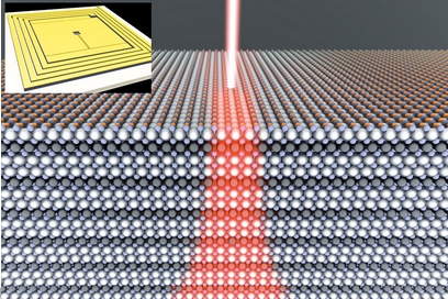
Working with research partner Carl Zeiss Microscopy LLC’s finely focused helium beam, “Orion,” the group, which also includes Tristan Technologies Inc., irradiated and disordered a nanoscale region of a superconductor to create a quantum mechanical tunnel barrier. They were then able to write Josephson circuits directly into a thin oxide superconductor.
“By using this direct-write method, we were able to eliminate lithographic processing and now offer the promise of a pathway to quantum mechanical circuits operating at more practical temperatures,” explained Shane Cybart, co-author and principal investigator working within the Department of Physics at UC San Diego.
Taking a step back, what exactly are “Josephson junctions” and why are they so desirable? They’re the basic building block of superconducting electronics, and can be considered “analogous to transistors in semiconductor electronics,” Cybart said.
A Josephson junction is composed of “two superconducting electrodes separated by a very small distance -- about a billionth of a meter,” he added. “Josephson-based circuits called ‘superconducting quantum interference devices’ or ‘SQUIDs’ are used for detectors of extremely small magnetic fields -- more than 10 billion times smaller than that of the Earth.”
One major drawback to devices from conventional materials is the low temperatures required for their operation -- typically just 4 degrees above absolute zero. “This requires intricate and costly cooling systems that use several thousand Watts,” Cybart said.
The key to the group’s direct-write method is that oxide superconductors are very sensitive to point defects in the crystal lattice caused by ion irradiation. “Increasing irradiation levels increases resistivity, while reducing the superconducting transition temperature,” Cybart said. “At very high irradiation levels, the superconductor becomes insulating and no longer conducts or superconducts, which allows us to use the small helium beam to directly write junctions into the material.” The diameter of the beam is comparable to the atomic spacing in the material.
While developing their direct-write approach, Cybart and colleagues encountered three substantial -- and pleasant -- surprises. The first was that while other researchers have used the irradiation method for making Josephson devices for many years, they were unable to make the features small enough for devices with a high figure of merit. “But we estimate that our group is producing devices with less than 2-nanometer dimensions, which results in ion irradiated devices that are about 100 times better in quality,” Cybart noted.
The second surprise was that although oxide SQUIDs are known to suffer from large magnetic field noise that limits their sensitivity, the group was able to demonstrate “very low noise characteristics similar to those of state-of-the-art SQUIDs.”
And the third surprise was the simplicity and ease of the entire process. “Current state-of-the-art high-transition-temperature SQUID sensors require many hours of difficult work to produce -- because each sensor is processed by hand, one at a time,” explained Cybart. “For about every 100 produced, only 10 have acceptable properties, which makes the cost around $10,000 per chip -- prohibitive for multi-sensor systems requiring hundreds of sensors. Our new technique allows for making hundreds of devices a day, so we expect it to slash costs and enable many applications previously considered too [expensive].”
In terms of potential applications, beyond the ability to manipulate these materials on a new length scale for fundamental studies, Cybart envisions near-term use in biomedical magnetic imaging equipment to noninvasively measure the tiny magnetic fields associated with neural activity in the brain, magneto enceptahalography (MEG). The next step for the group is a collaboration with medical researchers within the biomedical regime to build sensors for a liquid-nitrogen-based MEG system for studying neurological disorders such as autism and epilepsy in children.
Applications a bit further on the horizon include wide-bandwidth communications and high-performance computing. “Within the communications field, we’re developing wide-bandwidth, high-data throughput satellite communications,” said Cybart. “And for basic science, we’re using this technology to study ceramic superconducting materials to help determine the physics governing their operation that may lead to improved materials that work at even higher temperatures.”
Share on:


Suggested Items
Warm Windows and Streamlined Skin Patches – IDTechEx Explores Flexible and Printed Electronics
04/26/2024 | IDTechExFlexible and printed electronics can be integrated into cars and homes to create modern aesthetics that are beneficial and easy to use. From luminous car controls to food labels that communicate the quality of food, the uses of this technology are endless and can upgrade many areas of everyday life.
Book Excerpt: The Printed Circuit Assembler’s Guide to... Factory Analytics
04/24/2024 | I-Connect007 Editorial TeamIn our fast-changing, deeply competitive, and margin-tight industry, factory analytics can be the key to unlocking untapped improvements to guarantee a thriving business. On top of that, electronics manufacturers are facing a tremendous burden to do more with less. If you don't already have a copy of this book, what follows is an excerpt from the introduction chapter of 'The Printed Circuit Assembler’s Guide to... Factory Analytics: Unlocking Efficiency Through Data Insights' to whet your appetite.
Listen Up! The Intricacies of PCB Drilling Detailed in New Podcast Episode
04/25/2024 | I-Connect007In episode 5 of the podcast series, On the Line With: Designing for Reality, Nolan Johnson and Matt Stevenson continue down the manufacturing process, this time focusing on the post-lamination drilling process for PCBs. Matt and Nolan delve into the intricacies of the PCB drilling process, highlighting the importance of hole quality, drill parameters, and design optimization to ensure smooth manufacturing. The conversation covers topics such as drill bit sizes, aspect ratios, vias, challenges in drilling, and ways to enhance efficiency in the drilling department.
Elevating PCB Design Engineering With IPC Programs
04/24/2024 | Cory Blaylock, IPCIn a monumental stride for the electronics manufacturing industry, IPC has successfully championed the recognition of the PCB Design Engineer as an official occupation by the U.S. Department of Labor (DOL). This pivotal achievement not only underscores the critical role of PCB design engineers within the technology landscape, but also marks the beginning of a transformative journey toward nurturing a robust, skilled workforce ready to propel our industry into the future.
Winner of The Science Show Rakett 69 Receives Incap Scholarship
04/24/2024 | IncapThe winner of the Rakett 69 science show, Andri Türkson, who stood out as an electronics enthusiast, received a scholarship from Incap Estonia, along with an internship opportunity in Saaremaa.