


 Happy’s Tech Talk #28: The Power Mesh Architecture for PCBs
 It’s Only Common Sense: Would You Join Your Own Company?
 The Chemical Connection: Reducing Etch System Water Usage, Part 2
Demonstrating Stretchable Conductor's Ability to Conduct
July 13, 2015 | University of Michigan RegentsEstimated reading time: 3 minutes
The art of paper cutting may slice through a roadblock on the way to flexible, stretchable electronics, a team of engineers and an artist at the University of Michigan has found.
In the future, a little bend in your smartphone might be considered a feature rather than a defect. An important component of future electronics that can be rolled up, folded or embedded in flexible objects is the stretchable conductor, which would make up components like wires and electrodes.
Conductors that stretch are difficult to design, and among those that are known, they either don't expand by much or the conductivity takes a nosedive when they do. By developing a conductor inspired by kirigami, the Japanese art of paper cutting, conductivity is sacrificed up front. The cuts become barriers to electrical conductivity, but when stretched, the conductors are steady performers.
"The kirigami method allows us to design the deformability of the conductive sheets, whereas before it was very Edisonian process with a lot of misses and not a lot of hits," said Nicholas Kotov, the Joseph B. and Florence V. Cejka Professor of Engineering, referring to Thomas Edison's trial-and-error approach to invention.
This is because when materials are stretched to the max, it's difficult to predict when and where rips will occur. However, if the tears are designed in a thoughtful way, the material's ability to stretch and recover becomes reliable.
It sounds simple, but until art and engineering came together with this project, no one had reported using kirigami to tackle the challenge of stretchable conductors. The results are presented in the latest edition of Nature Materials.
Matt Shlian, artist and lecturer in the U-M Stamps School of Art and Design, inspired the work with a sheet of paper cut to extend into a herringbone mesh when stretched.
The first prototype of the kirigami stretchable conductor was tracing paper covered in carbon nanotubes. The layout was very simple, with cuts like rows of dashes that opened to resemble a cheese grater.
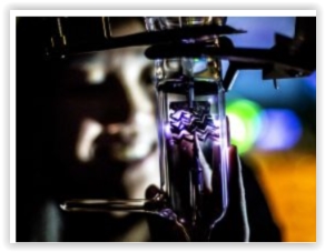
Rigged up in an argon-filled glass tube, the paper electrode turned the gas into a glowing plasma. The voltage across the electrode sent free electrons running into the argon atoms, causing them to emit light. Kotov explained that arrays of such electrodes could control the pixels of a stretchable plasma display.
The engineers wanted to understand exactly how design choices affected the behavior of the stretchable conductor, so Sharon Glotzer, the Stuart W. Churchill Professor of Chemical Engineering, and her research group, performed computer simulations.
"At first, computer simulation gave us intuition on what kinds of behaviors were to be expected from different cut patterns," said Pablo Damasceno, who recently earned his doctorate in applied physics.
Then, the simulation team explored how details like the length and curvature of the cuts, and the separation between them, related to the stretchiness of the material.
To produce the microscopic kirigami, Terry Shyu, a doctoral student in materials science and engineering, made special "paper" out of graphene oxide, a material composed of carbon and oxygen just one atom thick. She layered it with a flexible plastic, up to 30 layers of each.
The difficult part, she explained, was making the cuts just a few tenths of a millimeter long.
In the Lurie Nanofabrication Facility, she first coated the high-tech paper with a material that can be removed with laser light. She burned the dashes out of that material, which turned it into a mask for the etching process.
A plasma of oxygen ions and electrons broke down the "paper" that wasn't hidden under the mask, creating the neat rows of microscopic dashes. This material behaved as predicted by the simulations, stretching with no additional cost in conductivity.
Kotov is also a professor of chemical engineering, biomedical engineering, materials science and engineering and macromolecular science and engineering. Glotzer is also a professor of materials science and engineering, macromolecular science and engineering, physics, and applied physics.
The study was funded by the National Science Foundation.
Share on:


Suggested Items
Indium Corporation to Showcase HIA Materials at ECTC
05/07/2024 | Indium CorporationAs an industry leader in innovative materials solutions for semiconductor packaging and assembly, Indium Corporation® will feature its advanced products designed to meet the evolving challenges of heterogeneous integration and assembly (HIA) and fine-pitch system-in-package (SiP) applications at the 74th Electronic Components and Technology Conference (ECTC), May 28‒31, in Denver, Colorado.
Siemens Delivers New Solido IP Validation Suite
05/07/2024 | SiemensSiemens Digital Industries Software introduced Solido™ IP Validation Suite software, a comprehensive, automated signoff solution for quality assurance across all design intellectual property (IP) types, including standard cells, memories and IP blocks.
Altair Acquires Research in Flight, Forging a New Path for Aerodynamic Analysis
05/07/2024 | AltairAltair a global leader in computational intelligence, announced it has acquired Research in Flight, maker of FlightStream®, which provides computational fluid dynamics (CFD) software with a large footprint in the aerospace and defense sector and a growing presence in marine, energy, turbomachinery, and automotive applications.
Happy’s Tech Talk #28: The Power Mesh Architecture for PCBs
05/07/2024 | Happy Holden -- Column: Happy’s Tech TalkA significant decrease in HDI substrate production cost can be achieved by reducing the number of substrate layers from conventional through-hole multilayers and microvia multilayers of eight, 10, 12 (and more), down to four. Besides reducing direct processing steps, yield will increase as defect producing operations are eliminated.
Hirose Launches Solution Partner Network to Address Changing Design Challenges
05/06/2024 | HiroseHirose, a leader in the design and manufacturing of innovative connector solutions, has established a Solution Partner Network that enables OEMs to quickly explore product design, specialty IP, and component fulfillment options that best suit their needs.