


 It’s Only Common Sense: OCCAM—the Time Is Now
 Marcy's Musings: The Growing Industry
 Dan’s Biz Bookshelf: Seeing the How
Nanoscale Light-emitting Device has Big Profile
July 14, 2015 | University of Wisconsin-MadisonEstimated reading time: 2 minutes
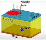
University of Wisconsin-Madison engineers have created a nanoscale device that can emit light as powerfully as an object 10,000 times its size. It's an advance that could have huge implications for everything from photography to solar power.
In a paper published July 10 in the journal Physical Review Letters,Zongfu Yu, an assistant professor of electrical and computer engineering, and his collaborators describe a nanoscale device that drastically surpasses previous technology in its ability to scatter light. They showed how a single nanoresonator can manipulate light to cast a very large "reflection." The nanoresonator's capacity to absorb and emit light energy is such that it can make itself — and, in applications, other very small things — appear 10,000 times as large as its physical size.
"Making an object look 10,000 times larger than its physical size has lots of implications in technologies related to light," Yu says.
The researchers realized the advance through materials innovation and a keen understanding of the physics of light. Much like sound, light can resonate, amplifying itself as the surrounding environment manipulates the physical properties of its wave energy. The researchers took advantage of this by creating an artificial material in which the wavelength of light is much larger than in a vacuum, which allows light waves to resonate more powerfully.
The device condenses light to a size smaller than its wavelength, meaning it can gather a lot of light energy, and then scatters the light over a very large area, harnessing its output for imaging applications that make microscopic particles appear huge.
"The device makes an object super-visible by enlarging its optical appearance with this super-strong scattering effect," says Ming Zhou, a Ph.D. student in Yu's group and lead author of the paper.
Much as a very thin string on a guitar can absorb a large amount of acoustic energy from its surroundings and begin to vibrate in sympathy, this one very small optical device can receive light energy from all around and yield a surprisingly strong output. In imaging, this presents clear advantages over conventional lenses, whose light-gathering capacity is limited by direction and size.
"We are developing photodetectors based on this technology and, for example, it could be helpful for photographers wanting to shoot better quality pictures in weak light conditions," Yu says.
Given the nanoresonator's capacity to absorb large amounts of light energy, the technology also has potential in applications that harvest the sun's energy with high efficiency. In addition, Yu envisions simply letting the resonator emit that energy in the form of infrared light toward the sky, which is very cold. Because the nanoresonator has a large optical cross-section — that is, an ability to emit light that dramatically exceeds its physical size — it can shed a lot of heat energy, making for a passive cooling system.
"This research opens up a new way to manipulate the flow of light, and could enable new technologies in light sensing and solar energy conversion," Yu says.
Zhou and Yu co-authored the Physical Review Letters paper with Lei Shi and Jian Zi of Fudan University in China. Yu's research is supported by the Office of Naval Research and the Wisconsin Alumni Research Foundation (WARF).
Share on:


Suggested Items
Inkjet Solder Mask ‘Has Arrived’
04/10/2024 | Pete Starkey, I-Connect007I was delighted to be invited to attend an interactive webinar entitled “Solder Mask Coating Made Easy with Additive Manufacturing,” hosted by SUSS MicroTec Netherlands in Eindhoven. The webinar was introduced and moderated by André Bodegom, managing director at Adeon Technologies, and the speakers were Mariana Van Dam, senior product manager PCB imaging solutions at AGFA in Belgium; Ashley Steers, sales manager at Electra Polymers in the UK; and Dr. Luca Gautero, product manager at SUSS MicroTec Netherlands.
NetVia Group Acquires Direct Imaging from Mivatek
04/09/2024 | Miva TechnologiesMiva Technologies is pleased to announce NetVia Group, Irving, TX has acquired a new Miva 2400NG Dual Tray Direct Imaging System with 30-micron capabilities for inner, outer and soldermask imaging.
Teledyne to Acquire Adimec
02/13/2024 | TeledyneTeledyne Technologies Incorporated announced that it has entered into an agreement to acquire Adimec Holding B.V. and its subsidiaries.
Real Time with... productronica 2023: MivaTek Global Advances Technology With High-res Imaging System
12/08/2023 | Real Time with...productronicaMivaTek's Brendan Hogan talks about how the company employs Digitally Adaptive Rasterization Technology (DART) in their high-res imaging equipment. He also shares how the blurred line between semiconductors and microelectronics is driving broader application of the imaging process.
Keysight Enables Validation of Arbe 4D Imaging Radar Chipset
11/30/2023 | Keysight Technologies, Inc.Keysight Technologies, Inc. announces that Arbe has selected the E8719A Radar Target Solution (RTS) to test the Arbe 4D imaging radar chipset for automotive applications.