


 Marcy's Musings: The Growing Industry
 It’s Only Common Sense: Here’s What To Do After IPC APEX EXPO 2024
 Dan’s Biz Bookshelf: Seeing the How
Compact Optical Data Transmission
August 4, 2015 | KITEstimated reading time: 3 minutes
Compact optical transmission possibilities are of great interest in faster and more energy-efficient data exchange between electronic chips. One component serving this application is the Mach-Zehnder modulator (MZM) which is able to convert electronic signals into optical signals. Scientists of the KIT and the ETH in Zurich developed a plasmonic MZM of only 12.5 micrometers length which converts digital electrical signals into optical signals at a rate of up to 108 gigabit per second, and presented this device in the “Nature Photonics” scientific journal.
“Optical technologies offer an enormous potential especially in transmitting data between computer chips,” explains Manfred Kohl of the KIT. The EU project he directs, NAVOLCHI, Nano Scale Disruptive Silicon-Plasmonic Platform for Chip-to-Chip Interconnection, developed the plasmonic modulator (an electric-to-optical converter) which is the basis of the current MZM. “Compact optical transmitter and receiver units could exceed the speed limits of present-day electronic systems and help get rid of the bottlenecks in data centers.”
The current publication presents an MZM only 12.5 micrometers long, which is roughly one tenth the thickness of a hair. It consists of two arms, each of which contains one electro-optical modulator. Each modulator is made up of a metal-insulator-metal waveguide with a gap approximately 80 nanometers wide and filled with an electro-optical polymer, and sidewalls made of gold which, at the same time, act as electrodes. The electrodes carry a voltage which is modulated in line with the digital data. The electro-optical polymer changes its index of refraction as a function of the voltage. The waveguide and the coupler made of silicon route the two parts of a split light beam to the gaps or from the gaps.
In the respective gap, the light beams of the waveguides initiate electromagnetic surface waves, the so-called surface plasmons. The voltage applied to the polymer modulates the surface waves. Modulation is different in both gaps but coherent, as the same voltage is applied with different polarities. After passing through the gaps, the surface waves initially enter the output optical waveguides as modulated light beams and are then superimposed. The result is a light beam in whose intensity (amplitude), the digital information was encoded.
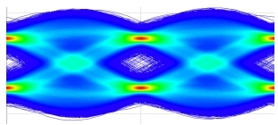
In the experiment, the MZM works reliably over the entire spectral range of the broad-band optical fiber networks of 1500 – 1600 nanometers at an electric bandwidth of 70 gigahertz with data flows of up to 108 gigabit per second. The large depth of modulation is a consequence of the high manufacturing accuracy in silicon technology. The MZM can also be made by means of the widespread CMOS-processes in microelectronics, and thus can easily be integrated into current chip architectures.
At the present time, some 10 percent of the electricity in Germany is consumed by information and communication technologies, such as computers and smart phones of users, but also by the servers in large computer centers. As data traffic grows exponentially, new approaches are necessary to increase throughput and, at the same time, curb power consumption. Plasmonic components could make a decisive contribution to this end.
The NAVOLCHI EU project serves to use the interaction of light and electrons in metal surfaces to develop novel components for optical data transmission between chips. The project is funded under the 7th Research Framework Programme of the European Union and has a budget of EUR 3.4 million.
About Karlsruhe Institute of Technology (KIT)
Karlsruhe Institute of Technology (KIT) is a public corporation pursuing the tasks of a state university of Baden-Wuerttemberg and of a national research center of the Helmholtz Association. The KIT mission combines the three core tasks of research, higher education, and innovation. With about 9,400 employees and 24,500 students, KIT is one of the big institutions of research and higher education in natural sciences and engineering in Europe.
Share on:


Suggested Items
D Coupon Testing and Data Insights With GreenSource Fabrication
04/17/2024 | Marcy LaRont, PCB007 MagazineMarcy LaRont spoke with Steve Karas of GreenSource Fabrication at the SMTA UHDI conference in March. He presented a case study that GreenSource undertook with a customer on critical via reliability with advanced materials and used the experience to highlight the importance and effectiveness of D coupon testing. He also discussed GreenSource’s approach to data aggregation and a new system they developed to use collected data effectively.
Real Time with... IPC APEX EXPO 2024: Innovations in Thermal, Warpage, and Strain Metrology
04/17/2024 | Real Time with...IPC APEX EXPOEditor Nolan Johnson talks with Neil Hubble, president of Akrometrix, about the company's leadership in thermal, warpage, and strain metrology. Neil details how Akrometrix is committed to addressing customer challenges through technological evolution, innovative solutions, and a focus on data processing. A tabletop unit for thermal warpage testing is showcased at IPC APEX EXPO this year.
Signal Integrity Expert Donald Telian to Teach 'Signal Integrity, In Practice' Masterclass Globally
04/17/2024 | PRLOGDonald Telian and The EEcosystem announce the global tour of "Signal Integrity, In Practice," a groundbreaking LIVE masterclass designed to equip hardware engineers with essential skills for solving Signal Integrity (SI) challenges in today's fast-paced technological landscape.
SMT Prospects and Perspectives: AI Opportunities, Challenges, and Possibilities, Part 1
04/17/2024 | Dr. Jennie Hwang -- Column: SMT Perspectives and ProspectsIn this installment of my artificial intelligence (AI) series, I will touch on the key foundational technologies that propel and drive the development and deployment of AI, with special consideration of electronics packaging and assembly.
Argonne, RIKEN Sign a Memorandum of Understanding in Support of AI for Science
04/16/2024 | BUSINESS WIRELeaders in high performance computing in the U.S. and Japan have signed a memorandum of understanding (MOU) establishing a cooperative relationship in support of artificial intelligence (AI) computing projects.