


 It’s Only Common Sense: OCCAM—the Time Is Now
 Marcy's Musings: The Growing Industry
 Dan’s Biz Bookshelf: Seeing the How
New Device Converts DC Electric Field to Terahertz Radiation
August 5, 2015 | AIP.orgEstimated reading time: 2 minutes
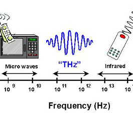
Terahertz radiation, the no-man's land of the electromagnetic spectrum, has long stymied researchers. Optical technologies can finagle light in the shorter-wavelength visible and infrared range, while electromagnetic techniques can manipulate longer-wavelength radiation like microwaves and radio waves. Terahertz radiation, on the other hand, lies in the gap between microwaves and infrared, whether neither traditional way to manipulate waves works effectively. As a result, creating coherent artificial sources of terahertz radiation in order to harness it for human use requires some ingenuity.
Difficulties of generating it aside, terahertz radiation has a wide variety of potential applications, particularly in medical and security fields. Because it's a non-ionizing form of radiation, it is generally considered safe to use on the human body. For instance, it can distinguish between tissues of different water content or density, making it a potentially valuable tool for identifying tumors. It could also be used to detect explosives or hidden weapons, or to wirelessly transmit data.
In a step towards more widespread use of terahertz radiation, researchers have designed a new device that can convert a DC electric field into a tunable source of terahertz radiation. Their results are published this week in the Journal of Applied Physics, from AIP Publishing.
This device exploits the instabilities in the oscillation of conducting electrons at the device's surface, a phenomenon known as surface plasmon resonance. To address the terahertz gap, the team created a hybrid semiconductor: a layer of thick conducting material paired with two thin, two-dimensional crystalline layers made from graphene, silicene (a graphene-like material made from silicon instead of carbon), or a two-dimensional electron gas. When a direct current is passed through the hybrid semiconductor, it creates a plasmon instability at a particular wavenumber. This instability induces the emission of terahertz radiation, which can be harnessed with the help of a surface grating that splits the radiation.
By adjusting various parameters -- such as the density of conduction electrons in the material or the strength of the DC electric field -- it is possible to tune the cutoff wavenumber and, consequently, the frequency of the resulting terahertz radiation.
"[Our work] demonstrates a new approach for efficient energy conversation from a dc electric field to coherent, high-power and electrically tunable terahertz emission by using hybrid semiconductors," said Andrii Iurov, a researcher with a dual appointment at the University of New Mexico's Center for High Technology Materials and the City University of New York. "Additionally, our proposed approach based on hybrid semiconductors can be generalized to include other novel two-dimensional materials, such as hexagonal boron nitride, molybdenum disulfide and tungsten diselenide."
Other labs have created artificial sources of terahertz radiation, but this design could enable better imaging capabilities than other sources can provide. "Our proposed devices can retain the terahertz frequency like other terahertz sources but with a much shorter wavelength for an improved spatial resolution in imaging application as well as a very wide frequency tuning range from a microwave to a terahertz wave," said Iurov.
The article, "Tunable surface plasmon instability leading to emission of radiation," is authored by Godfrey Gumbs, Andrii Iurov, Danhong Huang, and Wei Pan. It will appear in the Journal of Applied Physics on August 4, 2015. After that date, it can be accessed here.
The authors of this paper are affiliated with City University of New York, Donostia International Physics Center, Center for High Technology Materials at University of New Mexico, Air Force Research Laboratory and Sandia National Laboratory.
Share on:


Suggested Items
IDTechEx Report Unveils 3D Electronics Status and Opportunities
04/22/2024 | PRNewswire3D electronics is an emerging manufacturing approach that enables electronics to be integrated within or onto the surface of objects. 3D electronic manufacturing techniques empower new features, including mass customizability, greater integration, and improved sustainability in the electronics industry.
NASA, Japan Advance Space Cooperation, Sign Agreement for Lunar Rover
04/11/2024 | NASANASA Administrator Bill Nelson and Japan’s Minister of Education, Culture, Sports, Science and Technology (MEXT) Masahito Moriyama have signed an agreement to advance sustainable human exploration of the Moon.
Lockheed Martin Conducts Historic LRASM Flight Test
04/04/2024 | Lockheed MartinThe U.S. Navy in partnership with Lockheed Martin [NYSE: LMT] successfully conducted a historic Long-Range Anti-Ship Missile (LRASM) flight test with four missiles simultaneously in flight.
Ynvisible Appoints Felix Karlsson as Director
04/02/2024 | Ynvisible Interactive Inc.Ynvisible Interactive Inc. is pleased to announce the appointment of Felix Karlsson as a Director of the Company effective immediately.
Plasmatreat at IPC APEX EXPO 2024
04/02/2024 | PlasmatreatFor the pretreatment of highly sensitive electronic components, Plasmatreat will present a real innovation at the IPC APEX Expo in Anaheim 2024: The new REDOX tool safely and effectively reduces oxide layers on electronic components in an inline process.