


 It’s Only Common Sense: OCCAM—the Time Is Now
 Marcy's Musings: The Growing Industry
 Dan’s Biz Bookshelf: Seeing the How
Back to the Future: Next-Generation Vacuum Electronics
August 12, 2015 | DARPAEstimated reading time: 3 minutes
Solid-state electronics began to overtake vacuum tubes in radios, computers and other electronic and radio frequency gadgetry more than 60 years ago. Now we live in a Silicon Age. Even so, vacuum electronic devices, whose origins date to the 19th century, touch our lives every day.
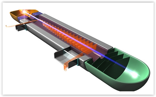
Those microwaves that heat the food in your microwave oven come from a magnetron, the vacuum tube that made radar possible in the first half of the 20th century. Traveling wave tubes (TWTs), not solid-state amplifiers, generate the strong electromagnetic signals in communication satellites because of their exceptional on-orbit reliability and high power efficiency. And it’s the unique ability of vacuum tube electronic devices to generate high-frequency signals at chip-melting operating powers that makes possible modern aviation radar systems for navigation and collision avoidance. What’s more, there are more than 200,000 vacuum electronic devices (VEDs) now in service in the Department of Defense, powering critical communications and radar systems that cover the land, sea, air, and space.
With its new Innovative Vacuum Electronic Science and Technology (INVEST) program, DARPA aims to develop the science and technology base for new generations of more capable VEDs.
“Any time you need to operate at the outer reaches of the power-frequency parameter space, vacuum tubes are the technology of choice,” said Dev Palmer, program manager for INVEST in DARPA’s Microsystems Technology Office (MTO). “But at the high millimeter-wave frequencies of interest to this program, the design and construction of VEDs is an intricate, labor-intensive process that requires exquisite modeling tools, exotic materials, and expensive, high-precision machining.” Physical scaling laws have been the showstopper for millimeter-wave VEDs so far: as engineers push the operating frequency of electronic devices upward, the output power from the same devices goes down. With INVEST, Palmer aims over the next four years to create a community of researchers that will find ways through this technical bottleneck.
Notwithstanding the popular notion that vacuum electronics are old-fashioned, the incentive to overcome technical and cost barriers to obtain next-generation VEDs is only getting stronger. “The worldwide availability and proliferation of inexpensive, high-power commercial amplifiers and sources has made the electromagnetic spectrum crowded and contested in the radio frequency (RF) and microwave regions,” according to MTO’s just-published Broad Agency Announcement (BAA), which invites the technical community to submit proposals for research that would take VED technology to new heights of power and frequency (DARPA-BAA-15-40, published on August 11, 2015, is available on FedBizOpps: http://go.usa.gov/3HqK9.)
VEDs capable of operating at higher frequencies and shorter wavelengths (in the millimeter wave region) than can outperform the current generation of devices will provide significant defense advantages. Higher power operation yields RF signals that are “louder” and thereby harder to jam and otherwise interfere with. Meanwhile, higher frequency operation brings with it vast swaths of previously unavailable spectrum. This too opens the way to more versatile communication, data transmission and other capabilities that will be beneficial in both military and civilian settings.
To open pathways towards those advances, the INVEST program aims to strengthen the science and technology base for new generations of vacuum tubes operating at millimeter-wave frequencies above 75 GHz. Those awarded contracts under the program will take on fundamental research projects in areas that include physics-based modeling and simulation of VEDs, innovative component design, electron emission processes, and advanced manufacturing. “As you push frequencies up, you can’t use conventional manufacturing techniques anymore,” Palmer said, pointing to the tiny size and ultraprecise alignment of millimeter-wave VED components, among them high-current-density cathodes, tiny vacuum envelopes, and microparts that extract the RF signals amplified inside the component.
“If you could print the whole structure with a 3-D printer, so that everything was aligned right off the assembly line, it would make it much easier,” Palmer says. Indeed, an ultimate and most welcome outcome would be to transform the new scientific understanding and engineering know-how that emerges from the INVEST program into novel tools for analyzing, synthesizing and optimizing new VED designs and then deploying innovative advanced manufacturing methods, including 3-D printing, to actually produce the devices. Said Palmer, “that is a beautiful vision.”
“Vacuum electronics is an infinitely deep subject,” added Palmer, whose fascination with the technology dates to his junior-high-school days in the 1970s when he was playing his electric guitar through the glowing vacuum tubes of his amplifier—something he continues to do today in his free time, with a continuing preference for tube-based amplifiers over solid state ones because of the subtle acoustical enhancements the “old” technology offers. “You have electromagnetics. You have high-temperature mechanical design. You have high-vacuum, magnetics, and materials science. It takes a choreographed effort across many disciplines to create one of these vacuum tubes.”
Share on:


Suggested Items
Nanotechnology Market to Surpass $53.51 Billion by 2031
04/25/2024 | PRNewswireSkyQuest projects that the nanotechnology market will attain a value of USD 53.51 billion by 2031, with a CAGR of 36.4% over the forecast period (2024-2031).
Cadence, TSMC Collaborate on Wide-Ranging Innovations to Transform System and Semiconductor Design
04/25/2024 | Cadence Design SystemsCadence Design Systems, Inc. and TSMC have extended their longstanding collaboration by announcing a broad range of innovative technology advancements to accelerate design, including developments ranging from 3D-IC and advanced process nodes to design IP and photonics.
SMC Korea 2024 to Highlight Semiconductor Materials Trends and Innovations on Industry’s Path to $1 Trillion
04/24/2024 | SEMIWith Korea a major consumer of semiconductor materials and advanced materials a key driver of innovation on the industry’s path to $1 trillion, industry leaders and experts will gather at SMC (Strategic Materials Conference) Korea 2024 on May 29 at the Suwon Convention Center in Gyeonggi-do, South Korea to provide insights into the latest materials developments and trends. Registration is open.
Orbex Secures £16.7m Investment for Rocket ‘Ramp Up’ Period
04/24/2024 | OrbexThe UK spaceflight company Orbex has received £16.7m from six backers in an update to its Series C funding round.
Real Time with... IPC APEX EXPO 2024: Going Vertical: SCHMID's Advanced Solutions for Printed Circuit Boards
04/24/2024 | Real Time with...IPC APEX EXPOEditor Marcy LaRont chats with Bob Ferguson, the president of SCHMID, about advanced solutions for PCBs and the equipment they are highlighting at this year's show. He delves into vertical no-touch handling systems and the prospect of achieving sub-10-micron lines. Inspired by SCHMID's technology, Bob expresses excitement about where the industry is today.