


 It’s Only Common Sense: OCCAM—the Time Is Now
 Marcy's Musings: The Growing Industry
 Dan’s Biz Bookshelf: Seeing the How
UT Researchers Give Nanosheets Local Magnetic Properties
September 10, 2015 | University of TwenteEstimated reading time: 3 minutes
Two-dimensional crystals are very suitable for creating high-quality magnetic thin films. This appears from two recent publications written by scientists from the University of Twente's MESA+ research institute. The researchers show that by growing the magnetic layers on various 2D crystals, better known as nanosheets, you can control the preferred direction of the magnetism very locally. In an article published in Advanced Functional Materials, they present this method to create magnetic patterns on the micrometer scale. In Angewandte Chemie, they demonstrate that you can make the nanosheets in less than a minute, while the synthesis process had been known to be very slow. The magnetic films can be deployed for many different applications, such as new generations of smartphones.
With pulsed laser deposition (PLD) you can achieve controlled growth of thin layers of certain materials. Here, a material is heated rapidly with a powerful laser beam, so that it evaporates and a plasma is created. This spreads quickly in a vacuum chamber and is deposited on a substrate where it forms a thin layer. In this way you can control the thickness of the layer and you can form smooth and thin layers, often with special properties that are interesting for use in electronics and electro-mechanics, for example. For such applications, it is however essential that you can also make patterns in the layered materials. This is not easy, especially because the substrate needs to be heated to temperatures above 500° C during the PLD process. Many of the existing methods are therefore not adapted to existing manufacturing methods for microstructures.
Use of nanosheets
The UT researchers have now developed a new method, in which they make use of nanosheets obtained from three-dimensional crystals with a layered structure. If you dissolve these crystals in a special liquid, they spontaneously disintegrate into individual nanosheets. It was long thought that the crystal disintegration process could take weeks. However, the researchers have now shown that the nanosheetsare already able to form within a few seconds, which opens the way for the production of nanosheets on a large scale.
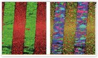
Based on the solution, various nanosheetscan be introduced in micro-patterns on a substrate. These patterns form the starting point for the growth of thin magnetic layers of magnetic LaSrMnO3 at high temperatures by means of PLD. Depending on the type of nanosheet the structure of the magnetic film assumes a specific orientation, and thus determines the magnetism of the film at that location. The process is monitored by means of, for example, electron backscatter diffraction (EBSD); a technique that makes it possible to 'reveal' the structure in the patterns.
Caption: EBSD image showing the local structure of a thin film. The left half of these images shows the preferred direction of the LaSrMnO3-film perpendicular to the growth direction, while the right half shows the directions in the plane with the contours of the individual nanosheets clearly visible. The distance between two lines in the pattern is a few micrometers.
Functional properties
The researchers show that you can use the micro patterns to control the functional properties of a material in detail. In addition to magnetism, it is possible to pattern other properties at the micrometer scale. An important step has thus been taking in bridging the gap between scientific research into artificial layered crystals and their ultimate application. The group from Twente plays a leading role in this worldwide.
Research
The research was performed by scientists from the Inorganic Materials Science department of UT research institute MESA+. It forms part of the TOP project funded by the Netherlands Organisation for Scientific Research (NWO) and the Chinese Scholarship Council. The research involved close cooperation with the Condensed-Matter and Medical Physics group at the University of California (UC, Irvine).
Share on:


Suggested Items
Koh Young Showcases Award-winning Inspection Solutions at SMTconnect with SmartRep in Hall 4A.225
04/25/2024 | Koh Young TechnologyKoh Young Technology, the industry leader in True 3D measurement-based inspection solutions, will showcase an array of award-winning inspection and measurement solutions at SMTconnect alongside its sales partner, SmartRep, in booth 4A.225 at NürnbergMesse from June 11-13, 2023. The following offers a glimpse into what Koh Young will present at the tradeshow:
Real Time with… IPC APEX EXPO 2024: Plasmatreat: Innovative Surface Preparation Solutions
04/25/2024 | Real Time with...IPC APEX EXPOIn this interview, Editor Nolan Johnson speaks with Hardev Grewal, CEO and president of Plasmatreat, a developer of atmospheric plasma solutions. Plasmatreat uses clean compressed air and electricity to create plasma, offering environmentally friendly methods for surface preparation. Their technology measures plasma density for process optimization and can remove organic micro-contamination. Nolan and Hardev also discuss REDOX-Tool, a new technology for removing metal oxides.
KYZEN to Promote Pair of Stencil Cleaning Chemistries at SMTA Ciudad Jaurez Expo & Tech Forum
04/25/2024 | KYZEN'KYZEN, the global leader in innovative environmentally friendly cleaning chemistries, will exhibit at the SMTA Ciudad Juarez Expo & Tech Forum, scheduled to take place Thursday, May 9, 2024 at the Injectronic Convention Center in Ciudad Jaurez, Chihuahua, Mexico. During the event the KYZEN Clean Team will focus on understencil cleaning products KYZEN E5631J and CYBERSOLV C8882.
Cadence, TSMC Collaborate on Wide-Ranging Innovations to Transform System and Semiconductor Design
04/25/2024 | Cadence Design SystemsCadence Design Systems, Inc. and TSMC have extended their longstanding collaboration by announcing a broad range of innovative technology advancements to accelerate design, including developments ranging from 3D-IC and advanced process nodes to design IP and photonics.
Listen Up! The Intricacies of PCB Drilling Detailed in New Podcast Episode
04/25/2024 | I-Connect007In episode 5 of the podcast series, On the Line With: Designing for Reality, Nolan Johnson and Matt Stevenson continue down the manufacturing process, this time focusing on the post-lamination drilling process for PCBs. Matt and Nolan delve into the intricacies of the PCB drilling process, highlighting the importance of hole quality, drill parameters, and design optimization to ensure smooth manufacturing. The conversation covers topics such as drill bit sizes, aspect ratios, vias, challenges in drilling, and ways to enhance efficiency in the drilling department.