


 It’s Only Common Sense: OCCAM—the Time Is Now
 Marcy's Musings: The Growing Industry
 Dan’s Biz Bookshelf: Seeing the How
Researchers See "Spin Current" in Motion for the First Time
September 11, 2015 | SLAC National Accelerator LaboratoryEstimated reading time: 3 minutes
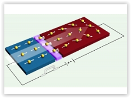
Researchers at the Department of Energy’s SLAC National Accelerator Laboratory have for the first time seen a spin current – an inherent magnetic property common to all electrons – as it travels across materials. The result, which revealed a surprising loss of current along the way, is an important step toward realizing a next-generation breed of electronics known as “spintronics.”.
Modern computing relies on the precise control of electric charges that zip around from component to component in labyrinth-like channels in semiconductors. Spintronics could change that by tapping electrons’ spin, which can be thought of as having an “up” or “down” orientation, rather than their charge.
Finding a way to directly control this up or down property, which is analogous to the magnetically stored zeros or ones in computer hard drive data, would rule out the need to flow electric charge in computer chips. Devices like laptops and smartphones would use less battery power and wouldn’t get so hot during use, and could also access data more quickly.
But the movement of this magnetic spin current had only been measured indirectly until a SLAC-led team found a way to directly observe it using X-rays. Their work, featured on the cover of the Aug. 28 edition of Physical Review Letters, could prove useful in guiding the selection of materials to improve spintronics performance.
Image - The Aug. 28, 2015, edition of Physical Review Letters features an illustration from a Stanford Synchrotron Radiation Lightsource scientific result.“It’s really a magnetic needle in a haystack,” said Hendrik Ohldag, a staff scientist at SLAC’s Stanford Synchrotron Radiation Lightsource (SSRL) who participated in the research. SSRL is a DOE Office of Science User Facility. The research team, which included researchers from industry, created a spintronics test device that flowed the spin current from a cobalt-based magnetic material across copper, a nonmagnetic material.
“What we really didn’t know was how this magnetization flowed from one material to another,” Ohldag said, “and that is what we saw for the first time.”
Simply seeing this spin-related current in the copper material was an important achievement, Ohldag said, but researchers also found that the current loses more than half of its magnetic spin strength as it travels from the magnetic material to the nonmagnetic material.
“We see that most of the magnetization gets lost here at the interface between the two materials,” added Roopali Kukreja, lead author of the paper and a graduate student at Stanford University at the time the experiments were performed. “This was an ‘Oh, wow!’ moment because nobody had suspected this. The copper atoms at the interface are almost magnetic, and that is where you really lose the spin property of this current. The role of this interface was not clear before.”
To make spintronics devices more effective for commercial applications, Ohldag said researchers will need to limit this loss of spin current at the interface between materials.
To isolate the magnetic spin property as it traveled from the magnet to copper, researchers worked with accelerator physicists and detector specialists at SLAC to customize a specialized microscope and detector system at SSRL. It could pick up the magnetic signal generated by as few as 50 atoms.
Ohldag said future experiments could use materials that are more promising for actual spintronic devices. “We can explore different materials and interfaces that are of different qualities and roughness,” he said.
Other participants in the research were from Stanford Institute for Materials and Energy Sciences (SIMES) at SLAC; Stanford University; New York University; Swiss Federal Institute of Technology; and HGST, a Western Digital Company. The work was supported by the DOE Office of Science, the National Science Foundation and the Knut and Alice Wallenberg Foundation.
Share on:


Suggested Items
Insulectro’s 'Storekeepers' Extend Their Welcome to Technology Village at IPC APEX EXPO
04/03/2024 | InsulectroInsulectro, the largest distributor of materials for use in the manufacture of PCBs and printed electronics, welcomes attendees to its TECHNOLOGY VILLAGE during this year’s IPC APEX EXPO at the Anaheim Convention Center, April 9-11, 2024.
ENNOVI Introduces a New Flexible Circuit Production Process for Low Voltage Connectivity in EV Battery Cell Contacting Systems
04/03/2024 | PRNewswireENNOVI, a mobility electrification solutions partner, introduces a more advanced and sustainable way of producing flexible circuits for low voltage signals in electric vehicle (EV) battery cell contacting systems.
Heavy Copper PCBs: Bridging the Gap Between Design and Fabrication, Part 1
04/01/2024 | Yash Sutariya, Saturn Electronics ServicesThey call me Sparky. This is due to my talent for getting shocked by a variety of voltages and because I cannot seem to keep my hands out of power control cabinets. While I do not have the time to throw the knife switch to the off position, that doesn’t stop me from sticking screwdrivers into the fuse boxes. In all honesty, I’m lucky to be alive. Fortunately, I also have a talent for building high-voltage heavy copper circuit boards. Since this is where I spend most of my time, I can guide you through some potential design for manufacturability (DFM) hazards you may encounter with heavy copper design.
Trouble in Your Tank: Supporting IC Substrates and Advanced Packaging, Part 5
03/19/2024 | Michael Carano -- Column: Trouble in Your TankDirect metallization systems based on conductive graphite or carbon dispersion are quickly gaining acceptance worldwide. Indeed, the environmental and productivity gains one can achieve with these processes are outstanding. In today’s highly competitive and litigious environment, direct metallization reduces costs associated with compliance, waste treatment, and legal issues related to chemical exposure. What makes these processes leaders in the direct metallization space?
AT&S Shines with Purest Copper on World Recycling Day
03/18/2024 | AT&SThe Styrian microelectronics specialist AT&S is taking World Recycling Day as an opportunity to review the progress that has been made in recent months at its sites around the world in terms of the efficient use of resources: