


 Marcy's Musings: The Growing Industry
 It’s Only Common Sense: Here’s What To Do After IPC APEX EXPO 2024
 Dan’s Biz Bookshelf: Seeing the How
Evidence of High-Temperature Superconductivity in Single Layer Unveiled
October 2, 2015 | ORNLEstimated reading time: 2 minutes
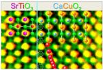
Electron microscopy at the Department of Energy’s Oak Ridge National Laboratory is pointing researchers closer to the development of ultra-thin materials that transfer electrons with no resistance at relatively high temperatures.
The study delivers direct evidence of high-temperature superconductivity at the interface of two insulating oxide materials. The paper by researchers from ORNL and the University of Rome Tor Vergata (Italy) is published in Physical Review Letters.
“One grand challenge in science is to manipulate materials locally by changing the distribution of atoms and the electronic structure, and that’s what we’re doing here,” Cantoni said. “This is a way to control the material – by manipulating the oxygen to make this interface superconducting.”
The ability to control and confine a material’s superconductivity could lead to two-dimensional superconductors for applications such as increasingly smaller computing technologies.
“We always want to scale down to get functionality in thinnest amount of material possible,” Cantoni said. “Usually when a material becomes thinner and thinner, its superconductivity disappears.”
In the PRL study, researchers used scanning transmission electron microscopy at ORNL to examine the interface between two insulators, calcium copper oxide and strontium titanate oxide. The resulting data, combined with electron energy loss spectroscopy, confirmed that high-temperature superconductivity occurs within a highly confined region around the interface.
“We were able to establish that a one-unit-cell-thick calcium copper oxide layer at this interface is superconducting and that the critical temperature approaches 50 Kelvin, which is considered high temperature superconductivity,” Cantoni said.
The team’s microscopy showed that superconductivity arises from oxygen ions that are incorporated into the interface calcium layer during the growth process. The extra oxygen ions pull electrons from the adjacent copper oxide layer, creating holes known to produce superconductivity.
The study is published as “High Tc superconductivity at the interface between the CaCuO2 and SrTiO3 insulating oxides.” Coauthors include University of Rome Tor Vergata’s D. Di Castro, F. Ridolfi, C. Aruta, A. Tebano, N. Yang, and G. Balestrino.
The research was supported in part by DOE’s Office of Science (Basic Energy Sciences) and used resources of the Center for Nanophase Materials Sciences, a DOE Office of Science User Facility at ORNL.
ORNL is managed by UT-Battelle for the Department of Energy’s Office of Science.
DOE’s Office of Science is the single largest supporter of basic research in the physical sciences in the United States, and is working to address some of the most pressing challenges of our time. For more information, please visit science.energy.gov.
Share on:


Suggested Items
Insulectro’s 'Storekeepers' Extend Their Welcome to Technology Village at IPC APEX EXPO
04/03/2024 | InsulectroInsulectro, the largest distributor of materials for use in the manufacture of PCBs and printed electronics, welcomes attendees to its TECHNOLOGY VILLAGE during this year’s IPC APEX EXPO at the Anaheim Convention Center, April 9-11, 2024.
ENNOVI Introduces a New Flexible Circuit Production Process for Low Voltage Connectivity in EV Battery Cell Contacting Systems
04/03/2024 | PRNewswireENNOVI, a mobility electrification solutions partner, introduces a more advanced and sustainable way of producing flexible circuits for low voltage signals in electric vehicle (EV) battery cell contacting systems.
Heavy Copper PCBs: Bridging the Gap Between Design and Fabrication, Part 1
04/01/2024 | Yash Sutariya, Saturn Electronics ServicesThey call me Sparky. This is due to my talent for getting shocked by a variety of voltages and because I cannot seem to keep my hands out of power control cabinets. While I do not have the time to throw the knife switch to the off position, that doesn’t stop me from sticking screwdrivers into the fuse boxes. In all honesty, I’m lucky to be alive. Fortunately, I also have a talent for building high-voltage heavy copper circuit boards. Since this is where I spend most of my time, I can guide you through some potential design for manufacturability (DFM) hazards you may encounter with heavy copper design.
Trouble in Your Tank: Supporting IC Substrates and Advanced Packaging, Part 5
03/19/2024 | Michael Carano -- Column: Trouble in Your TankDirect metallization systems based on conductive graphite or carbon dispersion are quickly gaining acceptance worldwide. Indeed, the environmental and productivity gains one can achieve with these processes are outstanding. In today’s highly competitive and litigious environment, direct metallization reduces costs associated with compliance, waste treatment, and legal issues related to chemical exposure. What makes these processes leaders in the direct metallization space?
AT&S Shines with Purest Copper on World Recycling Day
03/18/2024 | AT&SThe Styrian microelectronics specialist AT&S is taking World Recycling Day as an opportunity to review the progress that has been made in recent months at its sites around the world in terms of the efficient use of resources: