


 Marcy's Musings: The Growing Industry
 It’s Only Common Sense: Here’s What To Do After IPC APEX EXPO 2024
 Dan’s Biz Bookshelf: Seeing the How
Graphene Teams Up with 2D Crystals for Faster Data Communications
October 6, 2015 | ICFOEstimated reading time: 2 minutes
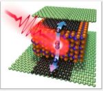
Ultra-fast detection of light lies at the heart of optical communication systems nowadays. Driven by the internet of things and 5G, data communication bandwidth is growing exponentially, thus requiring even faster optical detectors that can be integrated into photonic circuits.
In the recent work published today in Nature Nanotechnology, the research group led by Prof at ICFO Frank Koppens has shown that a two-dimensional crystal, combined with graphene, has the capability to detect optical pulses with a response faster than ten picoseconds, while maintaining a high efficiency. By using ultra-fast laser pulses, the researchers have shown a record-high photo-response speed for a heterostructure made of two-dimensional materials. These new materials are gaining more and more attention due to their amazing and rich variety of properties.
An important advantage of these devices based on graphene and other two-dimensional materials is that they can be integrated monolithically with silicon photonics enabling a new class of photonic integrated circuits. Although this study has been focused on the intrinsic properties of the photo-detection device, the next step is to develop prototype photonic circuitry and explore ways to improve large-scale production of these devices.
While Prof. Frank Koppens comments "It is remarkable how a material which is just a few nanometers thick can have such high performance", ICFO researcher Mathieu Massicotte and first author of this study states that "Everyone knew graphene could make ultrafast photodetectors, but related two-dimensional crystals were still lagging very much behind. In our work we show that by teaming up these two materials, we can obtain a photodetector that is not only ultrafast but also highly efficient."
The results obtained from this study have shown that the stacking of semiconducting 2D materials with graphene in heterostructures could lead to new, fast and efficient optoelectronic applications, such as high-speed integrated communication systems.
This study has been possible thanks to the support of the Fundació Cellex Barcelona, the European Research Council (ERC) and the EC under the Graphene Flagship, among others.
About ICFO
ICFO-The Institute of Photonic Sciences is a center of research excellence devoted to the science and technologies of light with a triple mission: to conduct frontier research, train the next generation of scientists, and provide knowledge and technology transfer.
Research at ICFO targets the forefront of science and technology based on light with programs directed at applications in Health, Renewable Energies, Information Technologies, Security and Industrial processes, among others. The institute hosts 300 professionals based in a dedicated building situated in the Mediterranean Technology Park in the metropolitan area of Barcelona.
ICFO participates in a large number of projects and international networks of excellence and is host to the NEST program financed by the Fundació Privada Cellex Barcelona. ICFO is a member of the Severo Ochoa Excelence program and a member of The Barcelona Institute of Science and Technology.
Share on:


Suggested Items
Absolute EMS Champions Collaboration Between Humans and Robots in Modern Manufacturing
04/19/2024 | Absolute EMS, Inc.Absolute EMS, Inc., an award-winning EMS provider of turnkey contract manufacturing services, offers a perfect factory environment that seamlessly blends robotic automation with human expertise.
Microsoft, Google Join as Sponsors for First-Ever AI Expo for National Competitiveness
04/19/2024 | SCSPThe Special Competitive Studies Project (SCSP), a non-partisan, non-profit project dedicated to strengthening America’s long-term competitiveness in artificial intelligence (AI), announced today two additional sponsors of the AI Expo for National Competitiveness.
IDTechEx Explores the Role of 3D Cu-Cu Hybrid Bonding in Powering Future HPC and AI Products
04/18/2024 | PRNewswireSemiconductor packaging has evolved from traditional 1D PCB levels to cutting-edge 3D hybrid bonding at the wafer level, achieving interconnecting pitches as small as single micrometers and over 1000 GB/s bandwidth. Key parameters, including Power, Performance, Area, and Cost, are crucial considerations
Intel Brings AI-Platform Innovation to Life at the Olympic Games
04/18/2024 | BUSINESS WIREIntel announced its plans for the Olympic and Paralympic Games Paris 2024. Bringing AI Everywhere, Intel will implement artificial intelligence technology powered by Intel processors on the world’s biggest stage.
Adura Solutions Exhibits at Del Mar 2024
04/18/2024 | Adura SolutionsSumit Tomar, CEO of Adura Solutions, has announced that his company will be exhibiting at this year's Del Mar Electronics and Manufacturing Show to be held at the Del Mar Fairgrounds, San Diego, California, April 24-25.