


 Marcy's Musings: The Growing Industry
 It’s Only Common Sense: Here’s What To Do After IPC APEX EXPO 2024
 Dan’s Biz Bookshelf: Seeing the How
Is Black Phosphorous the Next Big Thing in Materials?
October 19, 2015 | Lawrence Berkeley National LaboratoryEstimated reading time: 3 minutes
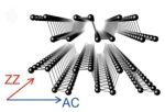
A new experimental revelation about black phosphorus nanoribbons should facilitate the future application of this highly promising material to electronic, optoelectronic and thermoelectric devices. A team of researchers at the U.S. Department of Energy (DOE)’s Lawrence Berkeley National Laboratory (Berkeley Lab) has experimentally confirmed strong in-plane anisotropy in thermal conductivity, up to a factor of two, along the zigzag and armchair directions of single-crystal black phosphorous nanoribbons.
“Imagine the lattice of black phosphorous as a two-dimensional network of balls connected with springs, in which the network is softer along one direction of the plane than another,” says Junqiao Wu, a physicist who holds joint appointments with Berkeley Lab’s Materials Sciences Division and the University of California (UC) Berkeley’s Department of Materials Science and Engineering. “Our study shows that in a similar manner heat flow in the black phosphorous nanoribbons can be very different along different directions in the plane. This thermal conductivity anisotropy has been predicted recently for 2D black phosphorous crystals by theorists but never before observed.”
Wu is the corresponding author of a paper describing this research in Nature Communications titled “Anisotropic in-plane thermal conductivity of black phosphorus nanoribbons at temperatures higher than 100K.” The lead authors are Sangwook Lee and Fan Yang. (See below for a complete list of authors)
Black phosphorous, named for its distinctive color, is a natural semiconductor with an energy bandgap that allows its electrical conductance to be switched “on and off.” It has been theorized that in contrast to graphene, black phosphorous has opposite anisotropy in thermal and electrical conductivities – i.e., heat flows more easily along a direction in which electricity flows with more difficultly. Such anisotropy would be a boost for designing energy-efficient transistors and thermoelectric devices, but experimental confirmation proved challenging because of sample preparation and measurement requirements.
“We fabricated black phosphorous nanoribbons in a top-down approach using lithography, then utilized suspended micro-pad devices to thermally isolate the nanoribbons from the environment so that tiny temperature gradient and thermal conduction along a single nanoribbon could be accurately determined,” Wu says. “We also went the extra mile to engineer the interface between the nanoribbon and the contact electrodes to ensure negligible thermal and electrical contact resistances, which is essential for this type of experiment.”
The results of the study, which was carried out at the Molecular Foundry, a DOE Office Science User Facility hosted by Berkeley Lab, revealed high directional anisotropy in thermal conductivity at temperatures greater than 100 Kelvin. This anisotropy was attributed mainly to phonon dispersion with some contribution from phonon-phonon scattering rate, both of which are orientation-dependent. Detailed analysis revealed that at 300 Kelvin, thermal conductivity decreased as the thickness of the nanoribbon thickness shrank from approximately 300 nanometers to approximately 50 nanometers. The anisotropy ratio remained at a factor of two within this thickness range.
“The anisotropy we discovered in the thermal conductivity of black phosphorous nanoribbons indicates that when these layered materials are patterned into different shapes for microelectronic and optoelectronic devices, the lattice orientation of the patterns should be considered,” Wu says. “This anisotropy can be especially advantageous if heat generation and dissipation play a role in the device operation. For example, these orientation-dependent thermal conductivities give us opportunities to design microelectronic devices with different lattice orientations for cooling and operating microchips. We could use efficient thermal management to reduce chip temperature and enhance chip performance.”
Wu and his colleagues plan to use their experimental platform to investigate how thermal conductivity in black phosphorous nanoribbons is affected under different scenarios, such as hetero-interfaces, phase-transitions and domain boundaries. They also want to explore the effects of various physical conditions such as stress and pressure.
This research was supported by the DOE Office of Science.
Share on:


Suggested Items
Real Time with... IPC APEX EXPO 2024: Exploring IPC's PCB Design Courses with Kris Moyer
04/18/2024 | Real Time with...IPC APEX EXPOGuest Editor Kelly Dack and IPC instructor Kris Moyer discuss IPC's PCB design training and education offerings. They delve into course topics such as design fundamentals, mil/aero, rigid-flex, RF design, and advanced design concepts. They also highlight material selection for high-speed design, thermal management, and dissipation techniques. The interview wraps up with details about how to access these courses online.
Adura Solutions Exhibits at Del Mar 2024
04/18/2024 | Adura SolutionsSumit Tomar, CEO of Adura Solutions, has announced that his company will be exhibiting at this year's Del Mar Electronics and Manufacturing Show to be held at the Del Mar Fairgrounds, San Diego, California, April 24-25.
Real Time with... IPC APEX EXPO 2024: Innovations in Thermal, Warpage, and Strain Metrology
04/17/2024 | Real Time with...IPC APEX EXPOEditor Nolan Johnson talks with Neil Hubble, president of Akrometrix, about the company's leadership in thermal, warpage, and strain metrology. Neil details how Akrometrix is committed to addressing customer challenges through technological evolution, innovative solutions, and a focus on data processing. A tabletop unit for thermal warpage testing is showcased at IPC APEX EXPO this year.
Hentec/RPS Publishes an Essential Guide to Selective Soldering Processing Tech Paper
04/17/2024 | Hentec Industries/RPS AutomationHentec Industries/RPS Automation, a leading manufacturer of selective soldering, lead tinning and solderability test equipment, announces that it has published a technical paper describing the critical process parameters that need to be optimized to ensure optimal results and guarantee the utmost in end-product quality.
Designing Electronics for High Thermal Loads
04/16/2024 | Akber Roy, Rush PCB Inc.Developing proactive thermal management strategies is important in the early stages of the PCB design cycle to minimize costly redesign iterations. Here, I delve into key aspects of electronic design that hold particular relevance for managing heat in electronic systems. Each of these considerations plays a pivotal role in enhancing the reliability and performance of the overall system.