


 Marcy's Musings: The Growing Industry
 It’s Only Common Sense: Here’s What To Do After IPC APEX EXPO 2024
 Dan’s Biz Bookshelf: Seeing the How
Nanotech Tools Open Market for More Miniature Electronics
October 29, 2015 | PICSEstimated reading time: 2 minutes
New methods for mass producing ultra-miniature capacitors could lead to new innovations in sectors ranging from medical tools to aeronautics.
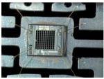
In order to develop ultra-miniaturised electronic components, ultra-miniaturised capacitors are required. The two-year EU-funded PICS project has developed tools that could soon lead to the mass production of high-density 3D integrated silicon capacitors, creating new opportunities for SMEs to tap demand for miniaturised high performance electronics across a range of sectors.
Capacitors are found in electronic components. Their role is to deliver power from a single source (such as a battery) – at the correct voltage level – in order for the component to carry out its different functions. Capacitors also protect electronic components against voltage jumps.
There is increasing demand from numerous high-growth high–value sectors, such as medicine, automotive, personal electronics and aeronautics, for applications based on smart and miniaturised sensors. These applications require electronic modules where size, reliability and performance are of equal importance.
The key long term objective of the project, which was completed at the end of August 2015, was to establish a cost effective industrial solution for developing ultra-miniaturised capacitors. Three SMEs joined forces with two research institutes in order to target the specific needs of end users such as aeronautics and medical instruments. Thanks to these partnerships, financial viability was ensured by focusing on the need for mass production.
Nanomedicine is another sector that is rapidly progressing from being primarily research-oriented to delivering measurable results and benefits to patients. The PICS consortium sought to develop high-end integrated capacitors for medical applications, along with the future DRAM market (DRAM is a type of random accessible memory used in various electronic devices such as PCs, smartphones, music players, laptops, netbooks, and tablets). The next step will be to commercially exploit the production innovations developed throughout the project.
A second long term objective of the project was to boost the potential of European SMEs operating within a high-value sector that promises significant growth potential. All three SMEs involved in PICS have benefited through the development of industry contacts and achieved a better understanding of end user needs. The project SMEs were also able to outsource some of their research in order to acquire cutting-edge technological know-how, which will enable them to better exploit their findings in the market place.
In terms of technological innovation, the project developed innovative atomic layer deposition (ALD) materials and tools in order to facilitate the mass production of high density and high voltage capacitors. ALD is a nanotechnology that allows ultra-thin films of just a few nanometres to be deposited in a precisely controlled way. This offers many benefits in semiconductor engineering. The tools developed by the PICS consortium enable 3D structures to be arranged.
A new process for accurately etching nanomaterials was also demonstrated by one of the SMEs, in collaboration with a leading research institute. This technique could be of interest for a number of different applications such as LED lighting and magnetic data storage.
Share on:


Suggested Items
IDTechEx Examines the Opportunities for Wearables in Digital Health
04/19/2024 | IDTechExIDTechEx’s report, “Digital Health and Artificial Intelligence 2024-2034: Trends, Opportunities, and Outlook”, covers this ongoing trend in the consumer health wearables market and includes analysis of the opportunities and roadmap for biometric monitoring.
Absolute EMS Champions Collaboration Between Humans and Robots in Modern Manufacturing
04/19/2024 | Absolute EMS, Inc.Absolute EMS, Inc., an award-winning EMS provider of turnkey contract manufacturing services, offers a perfect factory environment that seamlessly blends robotic automation with human expertise.
ZESTRON Welcomes Whitlock Associates as New Addition to their Existing Rep Team in Florida
04/19/2024 | ZESTRONZESTRON, the leading global provider of high-precision cleaning products, services, and training solutions in the electronics manufacturing and semiconductor industries, is thrilled to announce the addition of Whitlock Associates to its esteemed network of sales representatives.
IPC Bestows Posthumous Hall of Fame Award to Industry Icon Michael Ford
04/18/2024 | IPCIPC honored the late Michael Ford, Aegis Software, for his extraordinary contributions to the global electronics manufacturing industry with the IPC Raymond E. Pritchard Hall of Fame Award at IPC APEX EXPO 2024. IPC’s most prestigious honor, the Hall of Fame Award is given to individuals who have provided exceptional service and advancement to IPC and the electronics industry. Ford, an industry leader and valued IPC volunteer, died suddenly in January 2024.
SEMI Applauds U.S. Chips Act Award for Samsung Electronics Facilities to Strengthen Domestic Semiconductor Supply Chain
04/17/2024 | SEMISEMI, the industry association serving the global electronics design and manufacturing supply chain, applauded the United States Department of Commerce’s announcement of a Preliminary Memorandum of Terms for an award under the CHIPS and Science Act to support the expansion of Samsung Electronics’ presence in Texas and the company’s development and production of leading-edge chips.