


 Marcy's Musings: The Growing Industry
 It’s Only Common Sense: Here’s What To Do After IPC APEX EXPO 2024
 Dan’s Biz Bookshelf: Seeing the How
The Complexity of Modelling
November 4, 2015 | IUCREstimated reading time: 3 minutes
In recent years, advances in materials synthesis techniques have enabled scientists to produce increasingly complex functional materials with enhanced or novel macroscopic properties. For example, ultra-small core-shell metallic nanoparticles used for catalysis, high entropy alloys made of 6 or 7 elements to give high strength at high temperatures and pharmaceuticals engineered at the nano-scale for more effective drug delivery. Modern engineered materials drive progress in many scientific disciplines and are at the heart of next-generation technologies in industrial fields including electronics, energy production and storage, environmental engineering, and biomedicine. As the optical, electronic and mechanical properties of such materials are deeply influenced by atomic structure, solving the structure of engineered materials is of critical importance to unlocking their true potential.
However, the structures of such materials are often complex and non-periodic at the atomic scale or at the nanoscale. For example, many of the best known thermoelectric materials have structures that are crystallographic on average, but derive their high thermoelectric figure of merit from local atomic distortions. Disordered collections of nanoparticles, on the other hand, have a high degree of short- range order but no long-range order beyond the nanoscale. Additionally, many novel materials are composites, which exhibit complex ordering on multiple length scales, so the complexity faced by the materials scientist wishing to understand the structure of new and novel materials is considerable.
The standard techniques of crystallography have proven successful in characterizing a vast array of bulk materials whose atomic structures can be described with crystal models that require only tens or hundreds of parameters. Since X-ray diffraction data typically yield information on hundreds or thousands of diffraction peaks, a unique structure solution can almost always be found for crystalline materials. However, for the types of complex materials described above the number of degrees of freedom in suitable structure models is often considerably larger than in the case of a typical crystal. Additionally, complex engineered materials often produce extremely broad peaks in diffraction experiments, due to the fact that they are non-periodic or disordered. Thus, the structure problem is doubly complicated, as diffraction experiments produce less information than corresponding experiments on bulk materials. From a standard crystallographic perspective, the structure problem for many complex materials is inherently ill posed, making a unique solution impossible. When the standard techniques of crystallography fail, it is sometimes possible to develop new analytical tools to maximise the information extracted from a diffraction pattern, but even with such advances a unique solution can often not be found to a fundamentally ill-posed problem without defining new constraints or adding additional data.
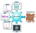
To obtain unique structure solutions for complex materials, a new paradigm of analysis is needed: a methodology that can combine different information sources and models into a coherent framework to solve problems using global optimisation. Within this framework, a material with unknown structure could be probed with various experimental tools, such as X-ray diffraction, transmission electron microscopy, small-angle X-ray or neutron scattering, Raman spectroscopy etc. to yield an array of data sets that would then be fed into a global optimiser. Additionally, theoretical inputs, such as density- functional theory could be integrated into the optimisation. While each single experimental or theoretical input may not generate enough information to produce a solution, together the pieces of information would regularise the problem, resulting in a unique solution.
A group of scientists from the United States of America [Juhás et al. (2015), Acta Cryst. A71, 562-568 provide a complete description of an implementation of complex modelling, one which is robust, modular and easily adaptable to different types of problems and different combinations of data sets and theoretical inputs. The key is to break the process down into its constituent parts, which can then be combined and linked as necessary to solve the problem at hand.
Share on:


Suggested Items
Groundbreaking Ceremony Marks the Beginning of a New Era for Newccess Industrial; The Construction of the MINGXIN Building
04/12/2024 | Newccess IndustrialOn a clear and sunny day in March, the groundbreaking ceremony for the MINGXIN Building took place in Shenzhen, China. This moment marked the official commencement of construction for a project that will reshape the semiconductor materials industry.
The Need for a Holistic Global Sustainability Standard
04/10/2024 | Michael Ford, Aegis SoftwareNo one can deny that the resources of our fragile planet are finite. The environment seems like a third party, subject to constant degradation. We’re acutely aware of the effects of pollution on our climate, and despite our “throw-away” culture, recycling and recovery of materials has remained relatively expensive, even as we use more energy just to survive.
iNEMI Publishes Four Roadmap Topics
04/04/2024 | iNEMIThe International Electronics Manufacturing Initiative (iNEMI) announces the availability of the first roadmap topics in the new iNEMI Roadmap format. Printed circuit boards, sustainable electronics, smart manufacturing, and mmWave materials and test are now available online.
Insulectro’s 'Storekeepers' Extend Their Welcome to Technology Village at IPC APEX EXPO
04/03/2024 | InsulectroInsulectro, the largest distributor of materials for use in the manufacture of PCBs and printed electronics, welcomes attendees to its TECHNOLOGY VILLAGE during this year’s IPC APEX EXPO at the Anaheim Convention Center, April 9-11, 2024.
Checking In With ICAPE Group
04/03/2024 | Nolan Johnson, I-Connect007ICAPE Group’s field application engineer Erik Pederson drills down on sustainability, supply chain resiliency, and what value engineering really looks like in this exclusive interview. Founded in 1999, European-based ICAPE Group provides 21 million printed circuit boards and over six million technical parts to manufacturers every month. With 30 PCB manufacturing partners globally and 50 partners providing a wide array of technical parts, ICAPE Group has operations in China, Taiwan, Thailand, South Korea, Vietnam, South Africa, Europe, Mexico, and the United States. The company also focuses on the value proposition for its customers.