


 It’s Only Common Sense: OCCAM—the Time Is Now
 Marcy's Musings: The Growing Industry
 Dan’s Biz Bookshelf: Seeing the How
New Electron Microscopy Method Sculpts 3-D Structures at Atomic Level
November 10, 2015 | Oak Ridge National LaboratoryEstimated reading time: 3 minutes
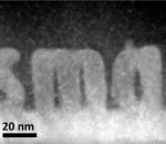
Electron microscopy researchers at the Department of Energy’s Oak Ridge National Laboratory have developed a unique way to build 3-D structures with finely controlled shapes as small as one to two billionths of a meter.
The ORNL study published in the journal Small demonstrates how scanning transmission electron microscopes, normally used as imaging tools, are also capable of precision sculpting of nanometer-sized 3-D features in complex oxide materials.
By offering single atomic plane precision, the technique could find uses in fabricating structures for functional nanoscale devices such as microchips. The structures grow epitaxially, or in perfect crystalline alignment, which ensures that the same electrical and mechanical properties extend throughout the whole material.
“We can make smaller things with more precise shapes,” said ORNL’s Albina Borisevich, who led the study. “The process is also epitaxial, which gives us much more pronounced control over properties than we could accomplish with other approaches.”
ORNL scientists happened upon the method as they were imaging an imperfectly prepared strontium titanate thin film. The sample, consisting of a crystalline substrate covered by an amorphous layer of the same material, transformed as the electron beam passed through it. A team from ORNL’s Institute for Functional Imaging of Materials, which unites scientists from different disciplines, worked together to understand and exploit the discovery.
“When we exposed the amorphous layer to an electron beam, we seemed to nudge it toward adopting its preferred crystalline state,” Borisevich said. “It does that exactly where the electron beam is.”
The use of a scanning transmission electron microscope, which passes an electron beam through a bulk material, sets the approach apart from lithography techniques that only pattern or manipulate a material’s surface.
“We’re using fine control of the beam to build something inside the solid itself,” said ORNL’s Stephen Jesse. “We’re making transformations that are buried deep within the structure. It would be like tunneling inside a mountain to build a house.”
The technique offers a shortcut to researchers interested in studying how materials’ characteristics change with thickness. Instead of imaging multiple samples of varying widths, scientists could use the microscopy method to add layers to the sample and simultaneously observe what happens.
“The whole premise of nanoscience is that sometimes when you shrink a material it exhibits properties that are very different than the bulk material,” Borisevich said. “Here we can control that. If we know there is a certain dependence on size, we can determine exactly where we want to be on that curve and go there.”
Theoretical calculations on ORNL’s Titan supercomputer helped the researchers understand the process’s underlying mechanisms. The simulations showed that the observed behavior, known as a knock-on process, is consistent with the electron beam transferring energy to individual atoms in the material rather than heating an area of the material.
“With the electron beam, we are injecting energy into the system and nudging where it would otherwise go by itself, given enough time,” Borisevich said. “Thermodynamically it wants to be crystalline, but this process takes a long time at room temperature.”
The study is published as “Atomic-level sculpting of crystalline oxides: towards bulk nanofabrication with single atomic plane precision.”
Coauthors are ORNL’s Stephen Jesse, Qian He, Andrew Lupini, Donovan Leonard, Raymond Unocic, Alexander Tselev, Miguel Fuentes-Cabrera, Bobby Sumpter, Sergei Kalinin and Albina Borisevich, Vanderbilt University’s Mark Oxley and Oleg Ovchinnikov and the National University of Singapore’s Stephen Pennycook.
The research was conducted as part of ORNL’s Institute for Functional Imaging of Materials and was supported by DOE’s Office of Science and ORNL’s Laboratory Directed Research and Development program. The study used resources at ORNL’s Center for Nanophase Materials Sciences and the Oak Ridge Leadership Computing Facility, which are both DOE Office of Science User Facilities.
ORNL is managed by UT-Battelle for the Department of Energy's Office of Science. DOE's Office of Science is the single largest supporter of basic research in the physical sciences in the United States, and is working to address some of the most pressing challenges of our time.
Share on:


Suggested Items
Groundbreaking Ceremony Marks the Beginning of a New Era for Newccess Industrial; The Construction of the MINGXIN Building
04/12/2024 | Newccess IndustrialOn a clear and sunny day in March, the groundbreaking ceremony for the MINGXIN Building took place in Shenzhen, China. This moment marked the official commencement of construction for a project that will reshape the semiconductor materials industry.
The Need for a Holistic Global Sustainability Standard
04/10/2024 | Michael Ford, Aegis SoftwareNo one can deny that the resources of our fragile planet are finite. The environment seems like a third party, subject to constant degradation. We’re acutely aware of the effects of pollution on our climate, and despite our “throw-away” culture, recycling and recovery of materials has remained relatively expensive, even as we use more energy just to survive.
iNEMI Publishes Four Roadmap Topics
04/04/2024 | iNEMIThe International Electronics Manufacturing Initiative (iNEMI) announces the availability of the first roadmap topics in the new iNEMI Roadmap format. Printed circuit boards, sustainable electronics, smart manufacturing, and mmWave materials and test are now available online.
Insulectro’s 'Storekeepers' Extend Their Welcome to Technology Village at IPC APEX EXPO
04/03/2024 | InsulectroInsulectro, the largest distributor of materials for use in the manufacture of PCBs and printed electronics, welcomes attendees to its TECHNOLOGY VILLAGE during this year’s IPC APEX EXPO at the Anaheim Convention Center, April 9-11, 2024.
Checking In With ICAPE Group
04/03/2024 | Nolan Johnson, I-Connect007ICAPE Group’s field application engineer Erik Pederson drills down on sustainability, supply chain resiliency, and what value engineering really looks like in this exclusive interview. Founded in 1999, European-based ICAPE Group provides 21 million printed circuit boards and over six million technical parts to manufacturers every month. With 30 PCB manufacturing partners globally and 50 partners providing a wide array of technical parts, ICAPE Group has operations in China, Taiwan, Thailand, South Korea, Vietnam, South Africa, Europe, Mexico, and the United States. The company also focuses on the value proposition for its customers.