


 The Right Approach: I Hear the Train A Comin'
 It’s Only Common Sense: OCCAM—the Time Is Now
 Marcy's Musings: The Growing Industry
New Approaches for Hybrid Solar Cells
December 8, 2015 | Technical University of MunichEstimated reading time: 3 minutes
Using a new procedure researchers at the Technical University of Munich (TUM) and the Ludwig Maximillians University of Munich (LMU) can now produce extremely thin and robust, yet highly porous semiconductor layers. A very promising material – for small, light-weight, flexible solar cells, for example, or electrodes improving the performance of rechargeable batteries.
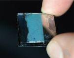
The coating on the wafer that Professor Thomas Fässler, chair of Inorganic Chemistry with a Focus on Novel Materials at TU Munich, holds in his hands glitters like an opal. And it has amazing properties: It is hard as a crystal, exceptionally thin and – since it is highly porous – light as a feather.
By integrating suitable organic polymers into the pores of the material, the scientists can custom tailor the electrical properties of the ensuing hybrid material. The design not only saves space, it also creates large interface surfaces that improve overall effectiveness.
“You can imagine our raw material as a porous scaffold with a structure akin to a honeycomb. The walls comprise inorganic, semiconducting germanium, which can produce and store electric charges. Since the honeycomb walls are extremely thin, charges can flow along short paths,” explains Fässler.
The new design: bottom-up instead of top-down
But, to transform brittle, hard germanium into a flexible and porous layer the researchers had to apply a few tricks. Traditionally, etching processes are used to structure the surface of germanium. However, this top-down approach is difficult to control on an atomic level. The new procedure solves this problem.
Together with his team, Fässler established a synthesis methodology to fabricate the desired structures very precisely and reproducibly. The raw material is germanium with atoms arranged in clusters of nine. Since these clusters are electrically charged, they repel each other as long as they are dissolved. Netting only takes place when the solvent is evaporated.
This can be easily achieved by applying heat of 500 °C or it can be chemically induced, by adding germanium chloride, for example. By using other chlorides like phosphorous chloride the germanium structures can be easily doped. This allows the researchers to directly adjust the properties of the resulting nanomaterials in a very targeted manner.
Page 1 of 2
Share on:


Suggested Items
SMC Korea 2024 to Highlight Semiconductor Materials Trends and Innovations on Industry’s Path to $1 Trillion
04/24/2024 | SEMIWith Korea a major consumer of semiconductor materials and advanced materials a key driver of innovation on the industry’s path to $1 trillion, industry leaders and experts will gather at SMC (Strategic Materials Conference) Korea 2024 on May 29 at the Suwon Convention Center in Gyeonggi-do, South Korea to provide insights into the latest materials developments and trends. Registration is open.
Groundbreaking Ceremony Marks the Beginning of a New Era for Newccess Industrial; The Construction of the MINGXIN Building
04/12/2024 | Newccess IndustrialOn a clear and sunny day in March, the groundbreaking ceremony for the MINGXIN Building took place in Shenzhen, China. This moment marked the official commencement of construction for a project that will reshape the semiconductor materials industry.
The Need for a Holistic Global Sustainability Standard
04/10/2024 | Michael Ford, Aegis SoftwareNo one can deny that the resources of our fragile planet are finite. The environment seems like a third party, subject to constant degradation. We’re acutely aware of the effects of pollution on our climate, and despite our “throw-away” culture, recycling and recovery of materials has remained relatively expensive, even as we use more energy just to survive.
iNEMI Publishes Four Roadmap Topics
04/04/2024 | iNEMIThe International Electronics Manufacturing Initiative (iNEMI) announces the availability of the first roadmap topics in the new iNEMI Roadmap format. Printed circuit boards, sustainable electronics, smart manufacturing, and mmWave materials and test are now available online.
Insulectro’s 'Storekeepers' Extend Their Welcome to Technology Village at IPC APEX EXPO
04/03/2024 | InsulectroInsulectro, the largest distributor of materials for use in the manufacture of PCBs and printed electronics, welcomes attendees to its TECHNOLOGY VILLAGE during this year’s IPC APEX EXPO at the Anaheim Convention Center, April 9-11, 2024.