


 The Right Approach: I Hear the Train A Comin'
 It’s Only Common Sense: OCCAM—the Time Is Now
 Marcy's Musings: The Growing Industry
Imec Improves Performance and Reliability of Deeply-scaled CMOS Logic Devices
December 9, 2015 | ImecEstimated reading time: 2 minutes
At IEEE International Electron Devices Meeting 2015, nano-electronics research center imec presented breakthrough results to increase performance and improve reliability of deeply scaled silicon CMOS logic devices.
Continued transistor scaling has resulted in increased transistor performance and transistor densities for the last 50 years. With transistor scaling reaching the critical limits of atomic dimensions, imec’s R&D program on advanced logic scaling targets the new and mounting challenges for performance, power, cost, and density scaling to future process technologies. Imec is looking into extending silicon CMOS technology by tackling the detrimental impact of parasitics on device performance and reliability, and by introducing novel architectures such as gate-all-around nanowires, that are considered to improve short channel control.
One of the achievements is a record low contact resistivity of 1.5 Ωcm2 for n-Si that was realized by combing dynamic surface anneal (DSA) to enhance P activation in highly-doped Si:P, with Ge pre-amorphisation and Ti silicidation. Imec also presented a decreased access resistance in NMOS Si bulk finFETs by applying extension doping by phosphorus doped silicate glass (PSG) to achieve damage free and uniform sidewall doping of the fin. Finally, imec introduced junction-less high-k metal-gate-all-around nanowires to improve on- and off-state hot carrier reliability.
“I am extremely proud with the record number of 23 papers that we present at this year’s IEDM2015,” stated Luc Van den hove, President and CEO at imec. “Our presence rewards and confirms our leading position in advanced semiconductor R&D. As much as 10 of the presented papers concerned the different aspects of our advanced logic program. Next to our research efforts to extend silicon CMOS technology into 7nm technology node and beyond. We are looking into beyond silicon CMOS, integrating high mobility materials to increase the channel mobility, and explore new concepts beyond silicon such as spintronics and 2D materials.”
Imec’s research into advanced logic scaling is performed in cooperation with imec’s key partners in its core CMOS programs including GlobalFoundries, Intel, Micron, Panasonic, Qualcomm, Samsung, SK Hynix, Sony and TSMC.
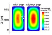
Cross-section of JL nanowires with or without an acceptor type interface, cut along the middle of the gate. The electrostatic potential is asymmetric when a trap is introduced; the squeezed channel improves the electrostatics and the subthreshold slope.
About imec
Imec performs world-leading research in nanoelectronics. Imec leverages its scientific knowledge with the innovative power of its global partnerships in ICT, healthcare and energy. Imec delivers industry-relevant technology solutions. In a unique high-tech environment, its international top talent is committed to providing the building blocks for a better life in a sustainable society. Imec is headquartered in Leuven, Belgium, and has offices in Belgium, the Netherlands, Taiwan, USA, China, India and Japan.Its staff of about 2,300 people includes almost 700 industrial residents and guest researchers. In 2014, imec's revenue (P&L) totaled 363 million euro.
Share on:


Suggested Items
Koh Young Showcases Award-winning Inspection Solutions at SMTconnect with SmartRep in Hall 4A.225
04/25/2024 | Koh Young TechnologyKoh Young Technology, the industry leader in True 3D measurement-based inspection solutions, will showcase an array of award-winning inspection and measurement solutions at SMTconnect alongside its sales partner, SmartRep, in booth 4A.225 at NürnbergMesse from June 11-13, 2023. The following offers a glimpse into what Koh Young will present at the tradeshow:
Real Time with… IPC APEX EXPO 2024: Plasmatreat: Innovative Surface Preparation Solutions
04/25/2024 | Real Time with...IPC APEX EXPOIn this interview, Editor Nolan Johnson speaks with Hardev Grewal, CEO and president of Plasmatreat, a developer of atmospheric plasma solutions. Plasmatreat uses clean compressed air and electricity to create plasma, offering environmentally friendly methods for surface preparation. Their technology measures plasma density for process optimization and can remove organic micro-contamination. Nolan and Hardev also discuss REDOX-Tool, a new technology for removing metal oxides.
Nanotechnology Market to Surpass $53.51 Billion by 2031
04/25/2024 | PRNewswireSkyQuest projects that the nanotechnology market will attain a value of USD 53.51 billion by 2031, with a CAGR of 36.4% over the forecast period (2024-2031).
Cadence, TSMC Collaborate on Wide-Ranging Innovations to Transform System and Semiconductor Design
04/25/2024 | Cadence Design SystemsCadence Design Systems, Inc. and TSMC have extended their longstanding collaboration by announcing a broad range of innovative technology advancements to accelerate design, including developments ranging from 3D-IC and advanced process nodes to design IP and photonics.
SMC Korea 2024 to Highlight Semiconductor Materials Trends and Innovations on Industry’s Path to $1 Trillion
04/24/2024 | SEMIWith Korea a major consumer of semiconductor materials and advanced materials a key driver of innovation on the industry’s path to $1 trillion, industry leaders and experts will gather at SMC (Strategic Materials Conference) Korea 2024 on May 29 at the Suwon Convention Center in Gyeonggi-do, South Korea to provide insights into the latest materials developments and trends. Registration is open.