


 Marcy's Musings: The Growing Industry
 It’s Only Common Sense: Here’s What To Do After IPC APEX EXPO 2024
 Dan’s Biz Bookshelf: Seeing the How
Imec Advances 200mm GaN-on-Si Technology Closer to Manufacturing
December 15, 2015 | ImecEstimated reading time: 2 minutes
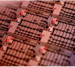
At IEEE International Electron Devices Meeting 2015, world-leading nano-electronics research center imec presented three novel aluminum gallium nitride (AlGaN)/ gallium nitride (GaN) stacks featuring optimized low dispersion buffer designs. Moreover, imec optimized the epitaxial p-GaN growth process on 200mm silicon wafers, achieving e-mode devices featuring beyond state-of-the-art high threshold voltage (Vt) and high drive current (Id).
To achieve a good, current-collapse-free device operation in AlGaN/GaN-on-Silicon (Si) devices, dispersion must be kept to a minimum. Trapped charges in the buffer between the GaN-based channel and the silicon substrate are known to be a critical factor in causing dispersion. Imec compared the impact of different types of buffers on dispersion and optimized three types: a classic step-graded buffer, a buffer with low-temperature AlN interlayers, and a super lattice buffer. These three types of buffers were optimized for low dispersion, leakage and breakdown voltage over a wide temperature range and bias conditions.
Imec also optimized the epitaxial p-GaN growth process demonstrating improved electrical performance of p-GaN HEMTs, achieving a beyond state-of-the-art combination of high threshold voltage, low on-resistance and high drive current (Vt >2V, RON= 7 Ω.mm and Id >0.4A/mm at 10V). The P-GaN HEMT results outperformed their MISHEMT counterparts.
Imec’s GaN-on-Si R&D program aims at bringing this technology towards industrialization. Imec’s offering includes a complete 200mm CMOS-compatible 200V GaN process line that features excellent specs on e-mode devices. Imec’s program allows partners early access to next-generation devices and power electronics processes, equipment and technologies, and speed up innovation at shared costs. Current R&D focuses on improving the performance and reliability of imec’s e-mode devices, while in parallel pushing the boundaries of the technology through innovation in substrate technology, higher levels of integration and exploration of novel device architectures.
“Imec’s presentations at the renowned IEDM meeting last week are a testament to the capabilities, sophistication, and maturity of our 200mm GaN-on-Silicon platform,” stated Rudi Cartuyvels, executive vice president of smart systems and energy technology at imec. “Building upon this success, we are now working with our GaN partners to implement and transfer specific device customizations. in parallel, we are exploring alternative substrate technologies to further push the boundaries of the GaN technology.”
About imec
Imec performs world-leading research in nanoelectronics. Imec leverages its scientific knowledge with the innovative power of its global partnerships in ICT, healthcare and energy. Imec delivers industry-relevant technology solutions. In a unique high-tech environment, its international top talent is committed to providing the building blocks for a better life in a sustainable society. Imec is headquartered in Leuven, Belgium, and has offices in Belgium, the Netherlands, Taiwan, USA, China, India and Japan. Its staff of about 2,300 people includes almost 700 industrial residents and guest researchers. In 2014, imec's revenue (P&L) totaled 363 million euro.
Share on:


Suggested Items
Absolute EMS Champions Collaboration Between Humans and Robots in Modern Manufacturing
04/19/2024 | Absolute EMS, Inc.Absolute EMS, Inc., an award-winning EMS provider of turnkey contract manufacturing services, offers a perfect factory environment that seamlessly blends robotic automation with human expertise.
Microsoft, Google Join as Sponsors for First-Ever AI Expo for National Competitiveness
04/19/2024 | SCSPThe Special Competitive Studies Project (SCSP), a non-partisan, non-profit project dedicated to strengthening America’s long-term competitiveness in artificial intelligence (AI), announced today two additional sponsors of the AI Expo for National Competitiveness.
IDTechEx Explores the Role of 3D Cu-Cu Hybrid Bonding in Powering Future HPC and AI Products
04/18/2024 | PRNewswireSemiconductor packaging has evolved from traditional 1D PCB levels to cutting-edge 3D hybrid bonding at the wafer level, achieving interconnecting pitches as small as single micrometers and over 1000 GB/s bandwidth. Key parameters, including Power, Performance, Area, and Cost, are crucial considerations
Intel Brings AI-Platform Innovation to Life at the Olympic Games
04/18/2024 | BUSINESS WIREIntel announced its plans for the Olympic and Paralympic Games Paris 2024. Bringing AI Everywhere, Intel will implement artificial intelligence technology powered by Intel processors on the world’s biggest stage.
Adura Solutions Exhibits at Del Mar 2024
04/18/2024 | Adura SolutionsSumit Tomar, CEO of Adura Solutions, has announced that his company will be exhibiting at this year's Del Mar Electronics and Manufacturing Show to be held at the Del Mar Fairgrounds, San Diego, California, April 24-25.