


 The Right Approach: I Hear the Train A Comin'
 It’s Only Common Sense: OCCAM—the Time Is Now
 Marcy's Musings: The Growing Industry
Nanoworld 'Snow Blowers' Carve Straight Channels in Semiconductor Surfaces
December 29, 2015 | NISTEstimated reading time: 2 minutes
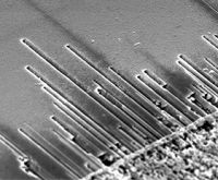
In the nanoworld, tiny particles of gold can operate like snow blowers, churning through surface layers of an important class of semiconductors to dig unerringly straight paths. The surprising trenching capability, reported by scientists from the National Institute of Standards and Technology (NIST) and IBM, is an important addition to the toolkit of nature-supplied “self-assembly” methods that researchers aim to harness for making useful devices.
Foreseeable applications include integrating lasers, sensors, wave guides and other optical components into so-called lab-on-a-chip devices now used for disease diagnosis, screening experimental materials and drugs, DNA forensics and more. Easy to control, the new gold-catalyzed process for creating patterns of channels with nanoscale dimensions could help to spawn entirely new technologies fashioned from ensembles of ultra-small structures.
Preliminary research results that began as lemons—a contaminant-caused failure that impeded the expected formation of nanowires—eventually turned into lemonade when scanning electron microscope images revealed long, straight channels.
“We were disappointed, at first,” says NIST research chemist Babak Nikoobakht. “Then we figured out that water was the contaminant in the process—a problem that turned out to be a good thing.”
That’s because, as determined in subsequent experiments, the addition of water vapor served to transform gold nanoparticles into channel diggers, rather than the expected wire makers. Beginning with studies on the semiconductor indium phosphide, the team teased out the chemical mechanisms and necessary conditions underpinning the surface-etching process.
First, they patterned the surface of the semiconductor by selectively coating it with a gold layer only a few nanometers thick. Upon heating, the film breaks up into tiny particles that become droplets. The underlying indium phosphide dissolves into the gold nanoparticles above, creating a gold alloy. Then, heated water vapor is introduced into the system. At temperatures below 300 degrees Celsius (572 degrees Fahrenheit), the tiny gold-alloy particles, now swathed with water molecules, etch nanoscale pits into the indium phosphide.
Page 1 of 2
Share on:


Suggested Items
Koh Young Showcases Award-winning Inspection Solutions at SMTconnect with SmartRep in Hall 4A.225
04/25/2024 | Koh Young TechnologyKoh Young Technology, the industry leader in True 3D measurement-based inspection solutions, will showcase an array of award-winning inspection and measurement solutions at SMTconnect alongside its sales partner, SmartRep, in booth 4A.225 at NürnbergMesse from June 11-13, 2023. The following offers a glimpse into what Koh Young will present at the tradeshow:
Real Time with… IPC APEX EXPO 2024: Plasmatreat: Innovative Surface Preparation Solutions
04/25/2024 | Real Time with...IPC APEX EXPOIn this interview, Editor Nolan Johnson speaks with Hardev Grewal, CEO and president of Plasmatreat, a developer of atmospheric plasma solutions. Plasmatreat uses clean compressed air and electricity to create plasma, offering environmentally friendly methods for surface preparation. Their technology measures plasma density for process optimization and can remove organic micro-contamination. Nolan and Hardev also discuss REDOX-Tool, a new technology for removing metal oxides.
KYZEN to Promote Pair of Stencil Cleaning Chemistries at SMTA Ciudad Jaurez Expo & Tech Forum
04/25/2024 | KYZEN'KYZEN, the global leader in innovative environmentally friendly cleaning chemistries, will exhibit at the SMTA Ciudad Juarez Expo & Tech Forum, scheduled to take place Thursday, May 9, 2024 at the Injectronic Convention Center in Ciudad Jaurez, Chihuahua, Mexico. During the event the KYZEN Clean Team will focus on understencil cleaning products KYZEN E5631J and CYBERSOLV C8882.
Cadence, TSMC Collaborate on Wide-Ranging Innovations to Transform System and Semiconductor Design
04/25/2024 | Cadence Design SystemsCadence Design Systems, Inc. and TSMC have extended their longstanding collaboration by announcing a broad range of innovative technology advancements to accelerate design, including developments ranging from 3D-IC and advanced process nodes to design IP and photonics.
Listen Up! The Intricacies of PCB Drilling Detailed in New Podcast Episode
04/25/2024 | I-Connect007In episode 5 of the podcast series, On the Line With: Designing for Reality, Nolan Johnson and Matt Stevenson continue down the manufacturing process, this time focusing on the post-lamination drilling process for PCBs. Matt and Nolan delve into the intricacies of the PCB drilling process, highlighting the importance of hole quality, drill parameters, and design optimization to ensure smooth manufacturing. The conversation covers topics such as drill bit sizes, aspect ratios, vias, challenges in drilling, and ways to enhance efficiency in the drilling department.