


 It’s Only Common Sense: OCCAM—the Time Is Now
 Marcy's Musings: The Growing Industry
 Dan’s Biz Bookshelf: Seeing the How
A New Metamaterial will Speed Up Computers
December 29, 2015 | Moscow Institute of Physics and TechnologyEstimated reading time: 4 minutes
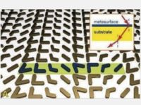
A team of scientists from the Moscow Institute of Physics and Technology (MIPT) and the Landau Institute for Theoretical Physics in the Russian Academy of Sciences has proposed a two-dimensional metamaterial composed of silver elements, that refracts light in an unusual way. The research has been published on Nov. 18, 2015 in Optical Material Express. In the future, these structures will be able to be used to develop compact optical devices, as well as to create an 'invisibility cloak.'
The results of computer simulations carried out by the authors showed that it would be a high performance material for light with a wavelength from 400-500nm (violet, blue and light blue). Efficiency in this case is defined as the percentage of light scattered in a desired direction. The efficiency of the material is approximately 70% for refraction, and 80% for reflection of the light. Theoretically, the efficiency could reach 100%, but in real metals there are losses due to ohm resistance.
A metamaterial is a material, the properties of which are created by an artificial periodic structure. The prefix 'meta' (from the Greek μετ? -- beyond) indicates that the characteristics of the material are beyond what we see in nature. Most often, when we talk about metamaterials, we mean materials with a negative refractive index. When light is incident on the surface of such a material, the refracted light is on the same side of the normal to the surface as the incident light. The difference between the behaviour of the light in a medium with a positive and a negative refractive index can be seen, for example, when a rod is immersed in liquid.
The existence of substances with a negative refractive index was predicted as early as the middle of the 20th century. In 1976 Soviet physicist V.G. Veselago published an article that theoretically describes their properties, including an unusual refraction of light. The term 'metamaterials' for such substances was suggested by Roger Walser in 1999. The first samples of metamaterials were made from arrays of thin wires and only worked with microwave radiation.
Importantly, the unusual optical effects do not necessarily imply the use of the volumetric (3d) metamaterials. You can also manipulate the light with the help of two-dimensional structures -- so-called metasurfaces. In fact, it is a thin film composed of individual elements.
Page 1 of 2
Share on:


Suggested Items
Water Management in a Large Printed Circuit Board Manufacturer
04/15/2024 | Charles Nehrig, TTM TechnologiesTTM’s environmental management is grounded in its Environmental Statement and Environmental Policy, which promote measures that make for a more responsible environmental management process. Our management system helps TTM work toward minimizing its environmental footprint and increasing the sustainability of its operations. TTM monitors its environmental performance just as it monitors its operational performance, and provides the resources required to adhere to the Company’s environmental responsibilities.
Happy’s Tech Talk #27: Integrated Mesh Power System (IMPS) for PCBs
04/08/2024 | Happy Holden -- Column: Happy’s Tech TalkA significant decrease in HDI substrate production cost can be achieved by reducing the number of substrate layers from conventional through-hole multilayers and microvia multilayers of eight, 10, 12, and more to only two layers. Besides reducing direct processing steps, the yield will increase as defect-producing operations are eliminated. The integrated mesh power system (IMPS) was invented in the latter years of MCM-D use for thin-film fabrication. Those geometries fit today into our use of ultra HDI.
Trouble in Your Tank: Supporting IC Substrates and Advanced Packaging, Part 5
03/19/2024 | Michael Carano -- Column: Trouble in Your TankDirect metallization systems based on conductive graphite or carbon dispersion are quickly gaining acceptance worldwide. Indeed, the environmental and productivity gains one can achieve with these processes are outstanding. In today’s highly competitive and litigious environment, direct metallization reduces costs associated with compliance, waste treatment, and legal issues related to chemical exposure. What makes these processes leaders in the direct metallization space?
Indium Corporation Experts to Present at SEMI THERM
03/07/2024 | Indium CorporationIndium Corporation Global Account Manager and Senior Thermal Technologist Tim Jensen and Product Development Specialist for Thermal Interface Materials Miloš Lazić will present on thermal interface material (TIM) technology at SEMI-THERM, taking place March 25–28 in San Jose, California, U.S.
Indium Corporation to Showcase Proven EV Products and High-Reliability Alloys at Productronica China
02/28/2024 | Indium CorporationAs a materials pioneer and trusted partner in electric vehicle (EV) and e-Mobility manufacturing, Indium Corporation is proud to showcase its high-reliability alloys and soldering solutions at Productronica China, March 20-22, in Shanghai.