


 It’s Only Common Sense: OCCAM—the Time Is Now
 Marcy's Musings: The Growing Industry
 Dan’s Biz Bookshelf: Seeing the How
Simultaneous Detection of the Polarities of Hundreds of Nanowires
January 4, 2016 | Universitat de ValènciaEstimated reading time: 2 minutes
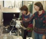
Researchers at the University of Valencia have developed a technique to determine the individual polarities of hundreds of semiconducting nanowires in a single, time-saving process. Led by Ana Cros, director of the University’s Materials Science Institute (ICMUV), the study constitutes a major step forward in both our understanding and application of these structures, since their polarity defines the properties of devices made from them.
Semiconducting nanowires are structures just tens of nanometres in diameter with a typical length-to-width ratio of around 1000 – like a human hair, only a thousand times smaller. So much so that they are often referred to as one-dimensional materials, and indeed they have many interesting properties not seen in larger 3D materials. Semiconducting nanowires are currently among the most-studied nanometric structures and are the basic building blocks for a range of optoelectronic devices that source, detect and control light, such as light detectors, emittors and nanosensors.
Until now, determining their polarities required the nanowires to be analysed one-by-one as part of a complex and time-consuming process. This new technique uses an atomic-strength microscope and a Kelvin probe to detect minuscule forces and measure the electrical characteristics of the sample’s surface. When combined with advanced data analysis, these measurements reveal the polarities of hundreds of nanowires at the same time.
Ana Cros offers us an analogy: “Our microscope explores the surface of the sample in the same way that a blind person explores their surroundings: it uses a probe as a cane, getting an idea as to surface properties based on changes in vibrations. The difference between the microscope and the cane is that its point is extremely sharp. If we then add the electrical charge, we are able to measure the electrical characteristics of the surface of very small objects without even needing to touch them.”
Known as Kelvin probe force microscopy (KPFM), this technique has made it possible to determine the individual polarities of over 100 nanowires at the same time. Núria Garro, researcher at the ICMUV, explains: “What used to take days -having to select the nanowires one-by-one and ultimately destroying the sample- now takes a matter of hours, without incurring any damage whatsoever to the sample”.
The study was published in the journal Nano Letters and was carried out jointly with the University of Murcia, the University of Grenoble and the French Atomic Energy Commission. It constitutes one of the primary findings from a new line of research opened at ICMUV for the study of optoelectronic processes in advanced materials and surfaces. It was carried out as part of the European NANOWIRING project (FP7-People).
Share on:


Suggested Items
Real Time with… IPC APEX EXPO 2024: Exploring the Future of Surface Finishes
04/25/2024 | Real Time with...IPC APEX EXPOJoe McGurran, product marketing director for MKS Atotech, looks into the future of surface finishes, discussing less nickel, reduced thickness, technologies influencing HDI and UHDI, and the benefits of nickel-free surface finishes. He also touches on popular finishes like ENIG and palladium immersion gold and discusses the value proposition of making a change.
Designer’s Notebook: What Designers Need to Know About Manufacturing, Part 2
04/24/2024 | Vern Solberg -- Column: Designer's NotebookThe printed circuit board (PCB) is the primary base element for providing the interconnect platform for mounting and electrically joining electronic components. When assessing PCB design complexity, first consider the component area and board area ratio. If the surface area for the component interface is restricted, it may justify adopting multilayer or multilayer sequential buildup (SBU) PCB fabrication to enable a more efficient sub-surface circuit interconnect.
IDTechEx Report Unveils 3D Electronics Status and Opportunities
04/22/2024 | PRNewswire3D electronics is an emerging manufacturing approach that enables electronics to be integrated within or onto the surface of objects. 3D electronic manufacturing techniques empower new features, including mass customizability, greater integration, and improved sustainability in the electronics industry.
NASA, Japan Advance Space Cooperation, Sign Agreement for Lunar Rover
04/11/2024 | NASANASA Administrator Bill Nelson and Japan’s Minister of Education, Culture, Sports, Science and Technology (MEXT) Masahito Moriyama have signed an agreement to advance sustainable human exploration of the Moon.
Lockheed Martin Conducts Historic LRASM Flight Test
04/04/2024 | Lockheed MartinThe U.S. Navy in partnership with Lockheed Martin [NYSE: LMT] successfully conducted a historic Long-Range Anti-Ship Missile (LRASM) flight test with four missiles simultaneously in flight.