


 It’s Only Common Sense: OCCAM—the Time Is Now
 Marcy's Musings: The Growing Industry
 Dan’s Biz Bookshelf: Seeing the How
Nanodevice, Build Thyself
January 15, 2016 | Alpha GalileoEstimated reading time: 3 minutes
Researchers in Germany studied how a multitude of electronic interactions govern the encounter between a molecule called porphine and copper and silver surfaces – information that could one day be harnessed to make molecular building blocks self-assemble into nanodevices.
As we continue to shrink electronic components, top-down manufacturing methods begin to approach a physical limit at the nanoscale. Rather than continue to chip away at this limit, one solution of interest involves using the bottom-up self-assembly of molecular building blocks to build nanoscale devices.
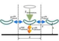
Successful self-assembly is an elaborately choreographed dance, in which the attractive and repulsive forces within molecules, between each molecule and its neighbors, and between molecules and the surface that supports them, have to all be taken into account. To better understand the self-assembly process, researchers at the Technical University of Munich have characterized the contributions of all interaction components, such as covalent bonding and van der Waals interactions between molecules and between molecules and a surface.
“In an ideal case, the smallest possible device has the size of a single atom or molecule,” said Katharina Diller, who worked as a postdoctoral researcher in the group of Karsten Reuter at the Technical University of Munich. Reuter and his colleagues present their work this week in The Journal of Chemical Physics, from AIP Publishing.
One such example is a single-porphyrin switch, which occupies a surface area of only one square nanometer. The porphine molecule, which was the object of this study, is even smaller than this. Porphyrins are a group of ringed chemical compounds which notably include heme – responsible for transporting oxygen and carbon dioxide in the bloodstream – and chlorophyll. In synthetically-derived applications, porphyrins are studied for their potential uses as sensors, light-sensitive dyes in organic solar cells, and molecular magnets.
Schematic depiction of different energy terms contributing to the adsorption energy, and charge density difference of 2H-P after adsorption onto Cu(111) at 12.8 Angstrom separation. Image Credit: M. Müller/TU Munich
Page 1 of 2
Share on:


Suggested Items
Designer’s Notebook: What Designers Need to Know About Manufacturing, Part 2
04/24/2024 | Vern Solberg -- Column: Designer's NotebookThe printed circuit board (PCB) is the primary base element for providing the interconnect platform for mounting and electrically joining electronic components. When assessing PCB design complexity, first consider the component area and board area ratio. If the surface area for the component interface is restricted, it may justify adopting multilayer or multilayer sequential buildup (SBU) PCB fabrication to enable a more efficient sub-surface circuit interconnect.
Insulectro’s 'Storekeepers' Extend Their Welcome to Technology Village at IPC APEX EXPO
04/03/2024 | InsulectroInsulectro, the largest distributor of materials for use in the manufacture of PCBs and printed electronics, welcomes attendees to its TECHNOLOGY VILLAGE during this year’s IPC APEX EXPO at the Anaheim Convention Center, April 9-11, 2024.
ENNOVI Introduces a New Flexible Circuit Production Process for Low Voltage Connectivity in EV Battery Cell Contacting Systems
04/03/2024 | PRNewswireENNOVI, a mobility electrification solutions partner, introduces a more advanced and sustainable way of producing flexible circuits for low voltage signals in electric vehicle (EV) battery cell contacting systems.
Heavy Copper PCBs: Bridging the Gap Between Design and Fabrication, Part 1
04/01/2024 | Yash Sutariya, Saturn Electronics ServicesThey call me Sparky. This is due to my talent for getting shocked by a variety of voltages and because I cannot seem to keep my hands out of power control cabinets. While I do not have the time to throw the knife switch to the off position, that doesn’t stop me from sticking screwdrivers into the fuse boxes. In all honesty, I’m lucky to be alive. Fortunately, I also have a talent for building high-voltage heavy copper circuit boards. Since this is where I spend most of my time, I can guide you through some potential design for manufacturability (DFM) hazards you may encounter with heavy copper design.
Trouble in Your Tank: Supporting IC Substrates and Advanced Packaging, Part 5
03/19/2024 | Michael Carano -- Column: Trouble in Your TankDirect metallization systems based on conductive graphite or carbon dispersion are quickly gaining acceptance worldwide. Indeed, the environmental and productivity gains one can achieve with these processes are outstanding. In today’s highly competitive and litigious environment, direct metallization reduces costs associated with compliance, waste treatment, and legal issues related to chemical exposure. What makes these processes leaders in the direct metallization space?