


 Marcy's Musings: The Growing Industry
 It’s Only Common Sense: Here’s What To Do After IPC APEX EXPO 2024
 Dan’s Biz Bookshelf: Seeing the How
Graphene Barrier to Precisely Control Molecules for Making Nanoelectronics
January 21, 2016 | UCLAEstimated reading time: 2 minutes
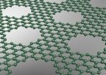
Gardeners often use sheets of plastic with strategically placed holes to allow their plants to grow but keep weeds from taking root.
Scientists from UCLA’s California NanoSystems Institute have found that the same basic approach is an effective way to place molecules in the specific patterns they need within tiny nanoelectronic devices. The technique could be useful in creating sensors that are small enough to record brain signals.
Led by Paul Weiss, a distinguished professor of chemistry and biochemistry, the researchers developed a sheet of graphene material with minuscule holes in it that they could then place on a gold substrate, a substance well suited for these devices. The holes allow molecules to attach to the gold exactly where the scientists want them, creating patterns that control the physical shape and electronic properties of devices that are 10,000 times smaller than the width of a human hair.
“We wanted to develop a mask to place molecules only where we wanted them on a stencil on the underlying gold substrate,” Weiss said. “We knew how to attach molecules to gold as a first step toward making the patterns we need for the electronic function of nanodevices. But the new step here was preventing the patterning on the gold in places where the graphene was. The exact placement of molecules enables us to determine exact patterning, which is key to our goal of building nanoelectronic devices like biosensors.”
With the advance, making nanoelectronic and nanobioelectronic devices could be much more efficient than current methods of molecular patterning, which use a technique called nanolithography. Weiss said that could be especially useful for scientists who are trying to place molecular sensors on the surface of gold or other nanomaterials that are used for their sensitivity and selectivity but difficult to work with because of their size.
Neurosensors that could measure brain cell and circuit function in real time could reveal new insights into diseases like autism and depression. Ultimately, Weiss said, the researchers hope to be able to stimulate individual brain circuits using sensors so they can predict key chemical differences between function and malfunction in the brain. This knowledge could then be used to develop targets for new generations of treatments for neurological diseases.
The paper’s other authors were John Thomas, Shan Jiang, Nathan Weiss and Xiangfeng Duan of UCLA, and Matthew Gethers and William Goddard III of Caltech.
Research for the study was conducted in the Electron Imaging Center for Nanomachines and the Nano and Pico Characterization Laboratory, which are both parts of the California NanoSystems Institute.
The research was supported by the U.S. Department of Energy, the National Science Foundation, the Caltech EAS Discovery Fund and UCLA.
Share on:


Suggested Items
Europlacer Announces Introductory Promotions for 2024 IPC APEX EXPO
03/27/2024 | EuroplacerEuroplacer, a leading provider of SMT assembly solutions, is excited to announce special introductory promotions for its latest products at the upcoming 2024 IPC APEX EXPO, scheduled to take place April 9-11, 2024 at the Anaheim Convention Center in California.
GEN3 to Demo SIR Testing, Stencil Cleaning & More with Horizon Sales at IPC APEX 2024
03/07/2024 | Gen3Gen3, global leader in SIR, CAF, Solderability, Ionic Contamination & process optimisation equipment, to announce its participation in the 2024 IPC APEX EXPO, scheduled to take place April 9-11, 2024 at the Anaheim Convention Center in California. At booth 3934, GEN3 will be exhibiting alongside Horizon Sales, presenting a lineup of advanced technologies aimed at enhancing the efficiency and reliability of circuit assembly processes.
AAT's Patented Rotational Spraying Method Ensures Superior Cleaning Performance
03/07/2024 | Austin American Technology (AAT)Austin American Technology (AAT) is pleased to announce that its patented rotational spraying method ensures superior cleaning performance, delivering consistent results for critical electronic components.
StenTech’s Photo Stencil Specialized Products Division Facility Update Completed
02/27/2024 | StenTechStenTech® Inc., a leading global company specializing in SMT Printing Solutions, has completed a major technology update to their Photo Stencil Specialized Products Division in Golden, Colorado. The phase-one overhaul included upgrades to key areas, including imaging, chemical plating, and chemical coating, along with refreshed offices and board room.
Stencil and PCB Cleaning Solutions from KYZEN at SMTA Monterrey
02/27/2024 | KyzenKYZEN, the global leader in innovative environmentally friendly cleaning chemistries, will exhibit at the SMTA Monterrey Expo & Tech Forum, scheduled to take place Thursday, March 14, 2024 at the Cintermex Convention Center, Hall 2A in Monterrey, Nuevo León. KYZEN will showcase the new aqueous chemistry AQUANOX A4618 in addition to highlighting stencil cleaning chemistries KYZEN E5631J and CYBERSOLV C8882.