


 It’s Only Common Sense: OCCAM—the Time Is Now
 Marcy's Musings: The Growing Industry
 Dan’s Biz Bookshelf: Seeing the How
Petawatt Laser System Passes a Key Milestone
January 25, 2016 | Lawrence Livermore National LaboratoryEstimated reading time: 3 minutes
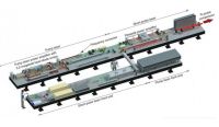
The High-Repetition-Rate Advanced Petawatt Laser System (HAPLS) under construction at LLNL recently achieved a key average power milestone more than two months ahead of schedule, and is now moving into the next phase in its development.
The HAPLS high-energy diode-pumped solid-state pump laser, firing at a repetition rate of 3.3 Hz (3.3 shots per second), achieved 70 joules of infrared (1,053-nanometer) energy and 39 joules of green (527-nm) energy. Completion of this average-power milestone marks another major step in the HAPLS commissioning plan: the beginning of the integration of the pump laser with the HAPLS high-energy short-pulse beamline.
“Ramping the pump laser to this intermediary performance level was an important step for HAPLS,” said Constantin Haefner, program director for Advanced Photon Technologies. “For the first time we ran the pump laser at significant energy and average power levels, meeting and exceeding the required goals for this milestone. This accomplishment required a huge team effort and the team worked extremely hard to make this happen.
“We are taking a risk-balanced approach in ramping HAPLS to its full performance. The data we collected confirmed our performance models and gave the green light to start integration with the short-pulse beamline before ramping to even higher power levels.”
Representatives from the European Union’s Extreme Light Infrastructure Beamlines (link is external) (ELI-Beamlines) facility in the Czech Republic, where HAPLS will be installed, attended the demonstration. “We are delighted to see the HAPLS pump laser work with a performance exceeding the project expectations for this phase, and achieve this important milestone on budget and ahead of schedule,” said ELI Beamlines Chief Laser Scientist Bedrich Rus. “The partnership with LLNL has been a tremendously successful story, and this demonstration shows the robustness of the underlying design and technology. The L3 (HAPLS) beamline will be an ELI Beamlines’ user facility workhorse.”
Page 1 of 2
Share on:


Suggested Items
Inkjet Solder Mask ‘Has Arrived’
04/10/2024 | Pete Starkey, I-Connect007I was delighted to be invited to attend an interactive webinar entitled “Solder Mask Coating Made Easy with Additive Manufacturing,” hosted by SUSS MicroTec Netherlands in Eindhoven. The webinar was introduced and moderated by André Bodegom, managing director at Adeon Technologies, and the speakers were Mariana Van Dam, senior product manager PCB imaging solutions at AGFA in Belgium; Ashley Steers, sales manager at Electra Polymers in the UK; and Dr. Luca Gautero, product manager at SUSS MicroTec Netherlands.
NetVia Group Acquires Direct Imaging from Mivatek
04/09/2024 | Miva TechnologiesMiva Technologies is pleased to announce NetVia Group, Irving, TX has acquired a new Miva 2400NG Dual Tray Direct Imaging System with 30-micron capabilities for inner, outer and soldermask imaging.
Teledyne to Acquire Adimec
02/13/2024 | TeledyneTeledyne Technologies Incorporated announced that it has entered into an agreement to acquire Adimec Holding B.V. and its subsidiaries.
Real Time with... productronica 2023: MivaTek Global Advances Technology With High-res Imaging System
12/08/2023 | Real Time with...productronicaMivaTek's Brendan Hogan talks about how the company employs Digitally Adaptive Rasterization Technology (DART) in their high-res imaging equipment. He also shares how the blurred line between semiconductors and microelectronics is driving broader application of the imaging process.
Keysight Enables Validation of Arbe 4D Imaging Radar Chipset
11/30/2023 | Keysight Technologies, Inc.Keysight Technologies, Inc. announces that Arbe has selected the E8719A Radar Target Solution (RTS) to test the Arbe 4D imaging radar chipset for automotive applications.