


 It’s Only Common Sense: OCCAM—the Time Is Now
 Marcy's Musings: The Growing Industry
 Dan’s Biz Bookshelf: Seeing the How
In Plasmonics, 'Optical Losses' Could Bring Practical Gain
January 27, 2016 | Purdue UniversityEstimated reading time: 2 minutes
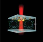
What researchers had thought of as a barrier to developing advanced technologies based on the emerging field of plasmonics is now seen as a potential pathway to practical applications in areas from cancer therapy to nanomanufacturing.
Plasmonic materials contain features, patterns or elements that enable unprecedented control of light by harnessing clouds of electrons called surface plasmons. It could allow the miniaturization of optical technologies, bringing advances such as nano-resolution imaging and computer chips that process and transmit data using light instead of electrons, representing a potential leap in performance.
However, the development of advanced optical technologies using plasmonics has been hampered because components under development cause too much light to be lost and converted into heat. But now researchers are finding that this "loss-induced plasmonic heating" could be key to development of various advanced technologies, said Vladimir M. Shalaev, co-director of the new Purdue Quantum Center, scientific director of nanophotonics at the Birck Nanotechnology Center in the university's Discovery Park and a distinguished professor of electrical and computer engineering.
The potential for practical applications using loss-induced plasmonic heating is discussed in a commentary that appeared on Jan. 22 in the Perspectives section of Science magazine. The article was written by doctoral student Justus Ndukaife, Shalaev and Alexandra Boltasseva, an associate professor of electrical and computer engineering.
"Plasmonics has generated significant interest because of the ability to squeeze light into nanoscale volumes in micro- and nano-devices, but progress has been hindered because of plasmonic losses," Ndukaife said. "We are saying we can use these losses to our advantage."
New technologies that could harness plasmonic heating include:
- A "nanotweezer" capable of positioning tiny objects quickly and accurately and freezing them in place, which could enable improved nanoscale sensing methods and aid research to manufacture advanced technologies such as quantum computers and ultra-high-resolution displays.
- A new magnetic storage technology called heat-assisted magnetic recording (HAMR), where nanoantennas, or near-field transducers, are used to focus light onto the magnetic medium. Nanoantennas could be leveraged in HAMR-based data storage. Moreover, plasmonic nanoparticles can be reshaped by heating and used to record images.
- Quadrapeutics, a clinical therapeutic approach using nanoparticles for cancer treatment. The nanoparticles are illuminated with laser light, producing plasmonic nanobubbles that can kill cancer cells.
- And a renewable energy concept that uses "plasmonic resonators" to improve the efficiency of solar cells.
"Harnessing the intrinsic loss in plasmonics could help to usher in transformative technological innovations affecting several fields, including information technology, life sciences and clean energy," Boltasseva said. "It is time for the plasmonic community to turn loss into gain."
Share on:


Suggested Items
Inkjet Solder Mask ‘Has Arrived’
04/10/2024 | Pete Starkey, I-Connect007I was delighted to be invited to attend an interactive webinar entitled “Solder Mask Coating Made Easy with Additive Manufacturing,” hosted by SUSS MicroTec Netherlands in Eindhoven. The webinar was introduced and moderated by André Bodegom, managing director at Adeon Technologies, and the speakers were Mariana Van Dam, senior product manager PCB imaging solutions at AGFA in Belgium; Ashley Steers, sales manager at Electra Polymers in the UK; and Dr. Luca Gautero, product manager at SUSS MicroTec Netherlands.
NetVia Group Acquires Direct Imaging from Mivatek
04/09/2024 | Miva TechnologiesMiva Technologies is pleased to announce NetVia Group, Irving, TX has acquired a new Miva 2400NG Dual Tray Direct Imaging System with 30-micron capabilities for inner, outer and soldermask imaging.
Teledyne to Acquire Adimec
02/13/2024 | TeledyneTeledyne Technologies Incorporated announced that it has entered into an agreement to acquire Adimec Holding B.V. and its subsidiaries.
Real Time with... productronica 2023: MivaTek Global Advances Technology With High-res Imaging System
12/08/2023 | Real Time with...productronicaMivaTek's Brendan Hogan talks about how the company employs Digitally Adaptive Rasterization Technology (DART) in their high-res imaging equipment. He also shares how the blurred line between semiconductors and microelectronics is driving broader application of the imaging process.
Keysight Enables Validation of Arbe 4D Imaging Radar Chipset
11/30/2023 | Keysight Technologies, Inc.Keysight Technologies, Inc. announces that Arbe has selected the E8719A Radar Target Solution (RTS) to test the Arbe 4D imaging radar chipset for automotive applications.