


 The Right Approach: I Hear the Train A Comin'
 It’s Only Common Sense: OCCAM—the Time Is Now
 Marcy's Musings: The Growing Industry
Novel Nanotechnology Technique for Table-Top Production of Flat Optics
January 28, 2016 | University of IllinoisEstimated reading time: 2 minutes
Researchers from the University of Illinois at Urbana-Champaign have developed a simplified approach to fabricating flat, ultrathin optics. The new approach enables simple etching without the use of acids or hazardous chemical etching agents.
“Our method brings us closer to making do-it-yourself optics a reality by greatly simplifying the design iteration steps,” explained Kimani Toussaint, an associate professor of mechanical science and engineering who led the research published this week in Nature Communications. “The process incorporates a nanostructured template that can be used to create many different types of optical components without the need to go into a cleanroom to make a new template each time a new optical component is needed.
“In recent years, the push to foster increased technological innovation and basic scientific and engineering interest from the broadest sectors of society has helped to accelerate the development of do-it-yourself (DIY) components, particularly those related to low-cost microcontroller boards,” Toussaint remarked. “Simplifying and reducing the steps between a basic design and fabrication is the primary attraction of DIY kits, but typically at the expense of quality. We present plasmon-assisted etching as an approach to extend the DIY theme to optics with only a modest tradeoff in quality, specifically, the table-top fabrication of planar optical components.”
“Our method uses the intuitive design aspects of diffractive optics by way of simple surface modification, and the electric-field enhancement properties of metal nanoantennas, which are typically the building blocks of metasurfaces,” stated Hao Chen, a former postdoctoral researcher in Toussaint’s lab and first author of the paper, “Towards do-it-yourself planar optical components using plasmon-assisted etching.”
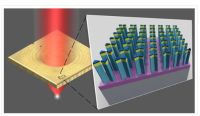
According to Chen, laser light scans the template—a 2D array of gold pillar-supported bowtie nanoantennas (with an area of 80 x 80 square micrometers)—which is submerged in water, in a desired pattern in a microscope. The light-matter interaction, enhanced by the nanoantennas, produces a strong heating effect. As a result, the gold layer of the nanoantennas undergoes thermal expansion that works against its adhesion with their glass substrate. With certain amount of optical power, the force provided by thermal expansion allows the gold layer to break away from the substrate, etching the metal.
“Overall, the workload in cleanroom is greatly reduced,” Chen noted. “Once the template is ready, it is like a paper sheet. You can ‘draw’ all the optical elements you need on a ‘canvas’ using a conventional laser-scanning optical microscope.”
The study demonstrated fabrication of various ultra-thin (characteristic dimension less than the optical wavelength), flat optical components using the same template. The specific optical components fabricated by the researchers included a flat focusing lens (also known as a Fresnel zone plate) with focal length of ~150 micrometers, a diffraction grating, and a holographic converter that imparts angular momentum to a standard optical beam.
According to the researchers, the PAE method and specialized template could also be used to enable preferential trapping and sorting of particles, to create so-called optofluidic channels “without walls.”
Toussaint directs the PROBE laboratory in the Department of Mechanical Science and Engineering at Illinois. In addition to Toussaint and Chen, study co-authors include graduate student Qing Ding, former graduate student Abdul Bhuiya, and Harley T. Johnson, a professor of mechanical science and engineering at Illinois.
Share on:


Suggested Items
Boeing Opens Research & Technology Center in Japan
04/23/2024 | BoeingBoeing today opened a Boeing Research & Technology (BR&T) Center in Japan that will focus on innovation to enable the commercial aviation industry meet its goal of net zero carbon emissions by 2050.
Ansys Joins BAE Systems’ Mission Advantage Program to Advance Digital Engineering Across US Department of Defense
04/16/2024 | ANSYSAnsys announced it is working with BAE Systems, Inc., to accelerate the adoption of digital engineering and MBSE across the Department of Defense (DoD).
Incap Estonia Teamed Up With Solaride to Fuel Youth Excitement for The World of Engineering
04/11/2024 | IncapIncap Estonia partnered with Solaride to ignite enthusiasm among young people for the world of engineering and sustainable technology. Together, they organised an inspiring day for students from grades 7 through 12 in Saaremaa. Held at Incap’s Kuressaare factory, this event brought together over 130 young minds eager to explore the innovative world of technology and learn more about advanced electronics manufacturing.
Mark Schulman Rocks Zuken Innovation World + integrate24
04/10/2024 | ZukenZuken USA, Inc. is excited to announce that the renowned drummer and motivational speaker, Mark Schulman, will be the keynote speaker at this year's Zuken Innovation World Americas (ZIW) conference, co-located with integrate24. Scheduled for September 17-19, 2024, in the vibrant city of Cleveland, Ohio, the conference aims to bring together the brightest minds in the PCB, Wire Harness, and Digital Engineering fields.
Saab Announces Plans for New Munitions Facility in U.S.
04/03/2024 | SaabSaab announced plans to build a new munitions facility in the U.S., continuing the company’s strong investment and growth domestically.