


 It’s Only Common Sense: OCCAM—the Time Is Now
 Marcy's Musings: The Growing Industry
 Dan’s Biz Bookshelf: Seeing the How
Ultrathin Semiconductor Heterostructures for New Technological Applications
February 15, 2016 | University of WashingtonEstimated reading time: 4 minutes
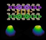
Heterostructures formed by different three-dimensional semiconductors form the foundation for modern electronic and photonic devices. Now, University of Washington scientists have successfully combined two different ultrathin semiconductors — each just one layer of atoms thick and roughly 100,000 times thinner than a human hair — to make a new two-dimensional heterostructure with potential uses in clean energy and optically-active electronics. The team, led by Boeing Distinguished Associate Professor Xiaodong Xu, announced its findings in a paper published Feb. 12 in the journal Science.
Senior author Xu and lead authors Kyle Seyler and Pasqual Rivera, both doctoral students in the UW physics department, synthesized and investigated the optical properties of this new type of semiconductor sandwich.
“What we’re seeing here is distinct from heterostructures made of 3-D semiconductors,” said Xu, who has joint appointments in the Department of Physics and the Department of Materials Science and Engineering. “We’ve created a system to study the special properties of these atomically thin layers and their potential to answer basic questions about physics and develop new electronic and photonic technologies.”
When semiconductors absorb light, pairs of positive and negative charges can form and bind together to create so-called excitons. Scientists have long studied how these excitons behave, but when they are squeezed down to the 2-D limit in these atomically thin materials, surprising interactions can occur.
While traditional semiconductors manipulate the flow of electron charge, this device allows excitons to be preserved in “valleys,” a concept from quantum mechanics similar to the spin of electrons. This is a critical step in the development of new nanoscale technologies that integrate light with electronics.
“It was already known that these ultrathin 2-D semiconductor have these unique properties that you cannot find in other 2-D or 3-D arrangements,” said Xu. “But as we show here, when we put these two layers together — one on top of the other — the interface between these sheets becomes the site of even more new physical properties, which you don’t see in each layer on its own or in the 3-D version.”
Xu and his team wanted to create and explore the properties of a 2-D semiconductor heterostructure made up of two different layers of material, a natural expansion of their previous studies on atomically thin junctions, as well as nanoscale lasers based on atomically thin layers of semiconductors. By studying how laser light interacts with this heterostructure, they gathered information about the physical properties at the atomically sharp interface.
“Many groups have studied the optical properties of single 2-D sheets,” said Seyler. “What we do here is carefully stack one material on top of another, and then study the new properties that arise at the interface.”
The team obtained two types of semiconducting crystals, tungsten diselenide (WSe2) and molybdenum diselenide (MoSe2), from collaborators at Oak Ridge National Laboratory. They used facilities developed in-house to precisely arrange two layers, one derived from each crystal, a process that took a few years to fully develop.
“But now that we know how to do it properly, we can make new ones in one or two weeks,” said Xu.
Getting these devices to emit light posed a unique challenge, due to the properties of electrons in each layer.
“Once you have these two sheets of material, an essential question is how to position the two layers together,” said Seyler. The electrons in each layer have unique spin and valley properties, and “how you position them — their twist angle — affects how they interact with light.”
By aligning the crystal lattices, the authors could excite the heterostructure with a laser and create optically active excitons between the two layers.
“These excitons at the interface can store valley information for orders of magnitude longer than either of the layers on their own,” said Rivera. “This long lifetime allows for fascinating effects which may lead to further optical and electronic applications with valley functionality.”
Now that they can efficiently make a semiconductor heterostructure out of 2-D materials, Xu and his team would like to explore a number of fascinating physical properties, including how exciton behavior varies as they change angles between the layers, the quantum properties excitons between layers and electrically driven light emission.
“There’s a whole industry that wants to use these 2-D semiconductors to make new electronic and photonic devices,” said Xu. “So we’re trying to study the fundamental properties of these new heterostructures for things like efficient laser technology, light-emitting diodes and light-harvesting devices. These will hopefully be useful for clean energy and information technology applications. It is quite exciting but there’s a lot work to do.”
Other co-authors are Hongyi Yu and Wang Yao at the University of Hong Kong; Jiaqiang Yan and David Mandrus at Oak Ridge National Laboratory and the University of Tennessee; and UW physics postdoctoral researcher John Schaibley. The UW authors were primarily funded by the U.S. Department of Energy, with additional support from the UW’s Clean Energy Institute and the National Science Foundation.
Share on:


Suggested Items
IDTechEx Report Unveils 3D Electronics Status and Opportunities
04/22/2024 | PRNewswire3D electronics is an emerging manufacturing approach that enables electronics to be integrated within or onto the surface of objects. 3D electronic manufacturing techniques empower new features, including mass customizability, greater integration, and improved sustainability in the electronics industry.
Incap Slovakia Supports Education With Classroom Equipment Sponsorship
02/26/2024 | IncapTo enhance the educational experience and foster innovation in teaching, Incap Slovakia has recently sponsored the purchase of an interactive board for the Ignác Gessay High School of Information Technology in Tvrdošín.
ROCKA Solutions Unveils New Website Design to Enhance Customer Experience
02/12/2024 | ROCKA SolutionsROCKA Solutions is excited to announce the launch of its redesigned website. The new website features a modern design aimed at improving the overall user experience and streamlining the inquiry and order process for customers.
Apollo Seiko Introduces the SR-LYRA II: A Fusion of Precision Soldering and High-Reliability SCARA Robot Technology
02/07/2024 | Apollo SeikoApollo Seiko, a leading innovator in soldering technology, proudly introduces the SR-LYRA II. This state-of-the-art soldering unit seamlessly combines the renowned LYRA II soldering technology with a highly-reliable SCARA robot, setting new standards for precision and efficiency in automated soldering processes.
Incap Estonia Supported Lümanda School With New Physics Teaching Tools
02/01/2024 | IncapIncap Estonia acquired educational kits for Lümanda School to support the development of future engineers. The new teaching tools are intended to enhance the teaching of natural sciences, especially physics.