


 It’s Only Common Sense: How to Win Back Lost Customers
 Punching Out: M&A North American PCB and EMS Deals for the First Half of 2025
 The Chemical Connection: Sales Organization from a Capital Equipment Perspective


Quantum Dot Solids: This Generation's Silicon Wafer?
February 25, 2016 | Cornell UniversityEstimated reading time: 3 minutes
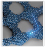
Just as the single-crystal silicon wafer forever changed the nature of electronics 60 years ago, a group of Cornell researchers is hoping its work with quantum dot solids – crystals made out of crystals – can help usher in a new era in electronics.
The multidisciplinary team, led by Tobias Hanrath, associate professor in the Robert Frederick Smith School of Chemical and Biomolecular Engineering, and graduate student Kevin Whitham, has fashioned two-dimensional superstructures out of single-crystal building blocks. Through directed assembly and attachment processes, the lead selenide quantum dots are synthesized into larger crystals, then fused together to form atomically coherent square superlattices.
The difference between these and previous crystalline structures is the atomic coherence of each 5-nanometer crystal (a nanometer is one-billionth of a meter). They’re not connected by a substance between each crystal – they’re connected directly to each other. The electrical properties of these superstructures potentially are superior to existing semiconductor quantum dots, with anticipated applications in solar cells and other electronic devices.
“As far as level of perfection, in terms of making the building blocks and connecting them into these superstructures, that is probably as far as you can push it,” Hanrath said, referring to the atomic-scale precision of the process.
The paper, “Charge transport and localization in atomically coherent quantum dot solids,” is published in the Feb. 22 issue of Nature Materials.
Whitham, a doctoral candidate in the field of materials science and engineering, did most of the experimentation and is lead author of the work. Also contributing were: Jun Yang, postdoctoral researcher; Benjamin H. Savitzky, graduate student in the field of physics; Lena Kourkoutis, assistant professor and Morgan Sesquicentennial Faculty Fellow in applied and engineering physics; and Frank Wise, the Samuel B. Eckert Professor of Engineering.
Provided
Associate professor Tobias Hanrath explains his group’s work on assembling quantum dots into ordered, two-dimensional superlattices, the subject of a paper published Feb. 22 in Nature Materials. The work has potential applications in optoelectronics.
This latest work has grown out of previous published research by the Hanrath group, including a 2013 paper published in Nano Letters that reported a new approach to connecting quantum dots through controlled displacement of a connector molecule, called a ligand. That paper referred to “connecting the dots” – i.e. electronically coupling each quantum dot – as being one of the most persistent hurdles to be overcome.
That barrier seems to have been cleared with this new research. The strong coupling of the quantum dots leads to formation of energy bands that can be manipulated based on the crystals’ makeup, and could be the first step toward discovering and developing other novel materials with programmable electronic structure.
Still, Whitham said, more work must be done to bring the group’s findings from the lab to technological fruition. The structure of the superlattice, while superior to ligand-connected quantum dot solids, still has multiple sources of disorder due to the fact that, in contrast to atoms in an ordinary solid, no two quantum dots are truly identical. This creates defects, which limits how far the electron wave function can spread.
“I see this paper as a challenge for other researchers to take this to another level,” Whitham said. “This is as far as we know how to push it now, but if someone were to come up with some technology, some chemistry, to provide another leap forward, this is challenging other people to say, ‘How can we do this better?’”
Hanrath said the discovery can be viewed in one of two ways, depending on whether you see the glass as half empty or half full.
“It’s the equivalent of saying, ‘Now we’ve made a really large single-crystal wafer of silicon, and access to high-quality samples yields new understanding and technological advances,’” he said, referencing the game-changing electronics discovery of the 1950s. “That’s the good part, but the potentially bad part of it is, we now have a better understanding that if you wanted to improve on our results, those challenges are going to be really, really difficult.”
This work made use of the Cornell Center for Materials Research, which is supported by the National Science Foundation (NSF) through its Materials Research Science and Engineering Center program. X-ray scattering was conducted at the Cornell High Energy Synchrotron Source, which is supported by the NSF and the National Institutes of Health.
Share on:


Testimonial
"The I-Connect007 team is outstanding—kind, responsive, and a true marketing partner. Their design team created fresh, eye-catching ads, and their editorial support polished our content to let our brand shine. Thank you all! "
Sweeney Ng - CEE PCBSuggested Items
Creating a Design Constraint Strategy
07/24/2025 | I-Connect007 Editorial TeamMost designers learn how to set their design constraints through trial and error. EDA vendors’ guidelines explain how to use their particular tools’ constraints, and IPC standards offer a roadmap, but PCB designers usually develop their own unique styles for setting constraints. Is there a set of best practices for setting constraints? That’s what I asked Global Electronics Association design instructor Kris Moyer, who covers design constraints in his classes.
Meet the Author: Beth Turner Explores Encapsulating Sustainability for Electronics
07/28/2025 | I-Connect007In a special Meet the Author edition of On the Line with…, host Nolan Johnson welcomes Beth Turner, senior technical manager at MacDermid Alpha Electronics Solutions. Beth is the author of The Printed Circuit Assembler’s Guide to… Encapsulating Sustainability for Electronics.
The Pulse: Design Constraints for the Next Generation
07/17/2025 | Martyn Gaudion -- Column: The PulseIn Europe, where engineering careers were once seen as unpopular and lacking street credibility, we have been witnessing a turnaround in the past few years. The industry is now welcoming a new cohort of designers and engineers as people are showing a newfound interest in the profession.
Copper Price Surge Raises Alarms for Electronics
07/15/2025 | Global Electronics Association Advocacy and Government Relations TeamThe copper market is experiencing major turbulence in the wake of U.S. President Donald Trump’s announcement of a 50% tariff on imported copper effective Aug. 1. Recent news reports, including from the New York Times, sent U.S. copper futures soaring to record highs, climbing nearly 13% in a single day as manufacturers braced for supply shocks and surging costs.
Symposium Review: Qnity, DuPont, and Insulectro Forge Ahead with Advanced Materials
07/02/2025 | Barb Hockaday, I-Connect007In a dynamic and informative Innovation Symposium hosted live and on Zoom on June 25, 2025, representatives from Qnity (DuPont's electronics business), DuPont, and Insulectro discussed the evolving landscape of flexible circuit materials. From strategic corporate changes to cutting-edge polymer films, the session offered deep insight into design challenges, reliability, and next-gen solutions shaping the electronics industry.