


 It’s Only Common Sense: OCCAM—the Time Is Now
 Marcy's Musings: The Growing Industry
 Dan’s Biz Bookshelf: Seeing the How
A Modified Device Fabrication Process Achieves Enhanced Spin Transport in Graphene
August 5, 2019 | ICN2Estimated reading time: 2 minutes
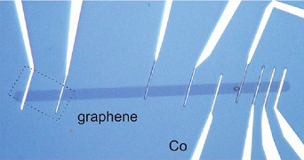
Researchers from the ICN2 Physics and Engineering of Nanodevices Group have proposed a modified graphene-based nanodevice fabrication technique that has increased up to three times the spin lifetime and relaxation length compared to previous work of the same kind. The work was fruit of the collaboration with Imec and K.U. Leuven (Belgium). The results have been published in 2D Materials and are expected to empower investigations on large-scale spintronic applications.
Spintronics is a field of research that was born in the 1980s. It amplifies the potential of traditional electronics by exploiting the electron’s spin degree of freedom, in addition to the usual state of charge. In the end, the goal is the same: to obtain devices to store, process and read information, but with enhanced characteristics such as lower power consumption, less heat dissipation, higher speed, etc. Although spintronics has not yet become as widespread as its conventional predecessor, some current devices are based on this new approach, such as magnetic hard disks, magnetic random access memories and magnetic sensors with varied applications in industrial environments, robotics and automotive industry.
Graphene is a promising material in this field. Spins can flow efficiently in it over long distances, meaning that they do not change their state (let’s say, from “up” to “down”) for a relatively long time. Due to its large-scale production, CVD graphene is becoming popular to fabricate spintronic devices. However, impurities arising from the graphene growth and device fabrication process limit its performance.
A team of scientists from the ICN2 Physics and Engineering of Nanodevices Group, led by ICREA Prof. Sergio O. Valenzuela, has proposed a high-yield device fabrication process from CVD graphene that has improved substantially its spin parameters. The work, whose first author is Zewdu M. Gebeyehu, was fruit of a collaboration with Imec and K.U. Leuven (Belgium). The results have been published in 2D Materials.
They demonstrate a spin signal measured across a 30 µm long channel with room-temperature spin lifetimes of up to 3 ns and spin relaxation lengths of up to 9 µm in monolayer graphene on SiO2/Si substrates. These spin parameters are the highest values for any form of graphene (both exfoliated and CVD graphene) on a standard SiO2/Si substrate.
To achieve this enhanced spin performance, the researchers used CVD graphene grown on a platinum foil and they modified the device fabrication technique so as to reduce the impurity levels associated with the graphene growth and fabrication steps. The latter requires the optimization of several standard processes, involving the preselection of high-quality uniform graphene with low level of impurities, an etching step combining e-beam lithography and oxygen plasma and a suitable post-annealing in high vacuum. The approach can be scaled and allows a highly reproducible fabrication of devices, which is the main requirement for potential industrialization.
The improvement on the spin parameters together with the reproducibility of the device fabrication process brings us closer to the realization of complex circuit architectures for spintronic devices such as spin logic and logic-in-memory for beyond CMOS computing.
Share on:


Suggested Items
Designer’s Notebook: What Designers Need to Know About Manufacturing, Part 2
04/24/2024 | Vern Solberg -- Column: Designer's NotebookThe printed circuit board (PCB) is the primary base element for providing the interconnect platform for mounting and electrically joining electronic components. When assessing PCB design complexity, first consider the component area and board area ratio. If the surface area for the component interface is restricted, it may justify adopting multilayer or multilayer sequential buildup (SBU) PCB fabrication to enable a more efficient sub-surface circuit interconnect.
Real Time with... IPC APEX EXPO 2024: Advancements in Laser Depaneling with LPKF
04/24/2024 | Real Time with...IPC APEX EXPOJake Benz, LPKF sales manager for North America, discusses the company's advancements in laser depaneling. LPKF has introduced a green wavelength laser for processing rigid FR-4 circuit boards, bringing significant gains in processing speeds to market. The company transitioned from IR CO2 to UV wavelength due to heat and burning issues.
KYZEN to Focus on AQUANOX A4618 at SMTA Wisconsin Expo & Tech Forum
04/22/2024 | KYZEN'KYZEN, the global leader in innovative environmentally friendly cleaning chemistries, will exhibit at the SMTA Wisconsin Expo & Tech Forum, scheduled to take place Tuesday, May 7, 2024 at the Four Poins by Sheraton, Milwaukee Airport in Milwaukee, WI.
AIM Solder’s Dillon Zhu to Present on Ultraminiature Soldering at SMTA China East
04/22/2024 | AIMAIM Solder, a leading global manufacturer of solder assembly materials for the electronics industry, is pleased to announce that Dillon Zhu will present on the topic: Ultraminiature Soldering: Techniques, Technologies, and Standards at SMTA China East. This event is being held at the Shanghai World Expo Exhibition & Convention Center from April 24-25.
Intel Gaudi, Xeon and AI PC Accelerate Meta Llama 3 GenAI Workloads
04/22/2024 | Intel CorporationMeta launched Meta Llama 3, its next-generation large language model (LLM). Effective on launch day, Intel has validated its AI product portfolio for the first Llama 3 8B and 70B models across Intel® Gaudi® accelerators, Intel® Xeon® processors, Intel® Core™ Ultra processors and Intel® Arc™ graphics.